Bad 8316 or something else

Hi everyone,

hope someone can help me like last time when I had to replace the P13USB. This time my nephew told me that he get no signal while in dock mode. So I opened it up and replaced the P13USB once more. First it didn’t work, because I guess the P13USB was off for one PIN on only one side (short side where the dot is). Now it looks good:

I did it again with the same chip and now dock mode works. But while assembling it and testing it several times I noticed that in handheld mode the LCD stays black.

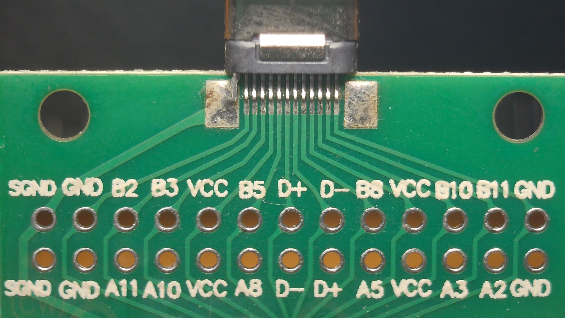
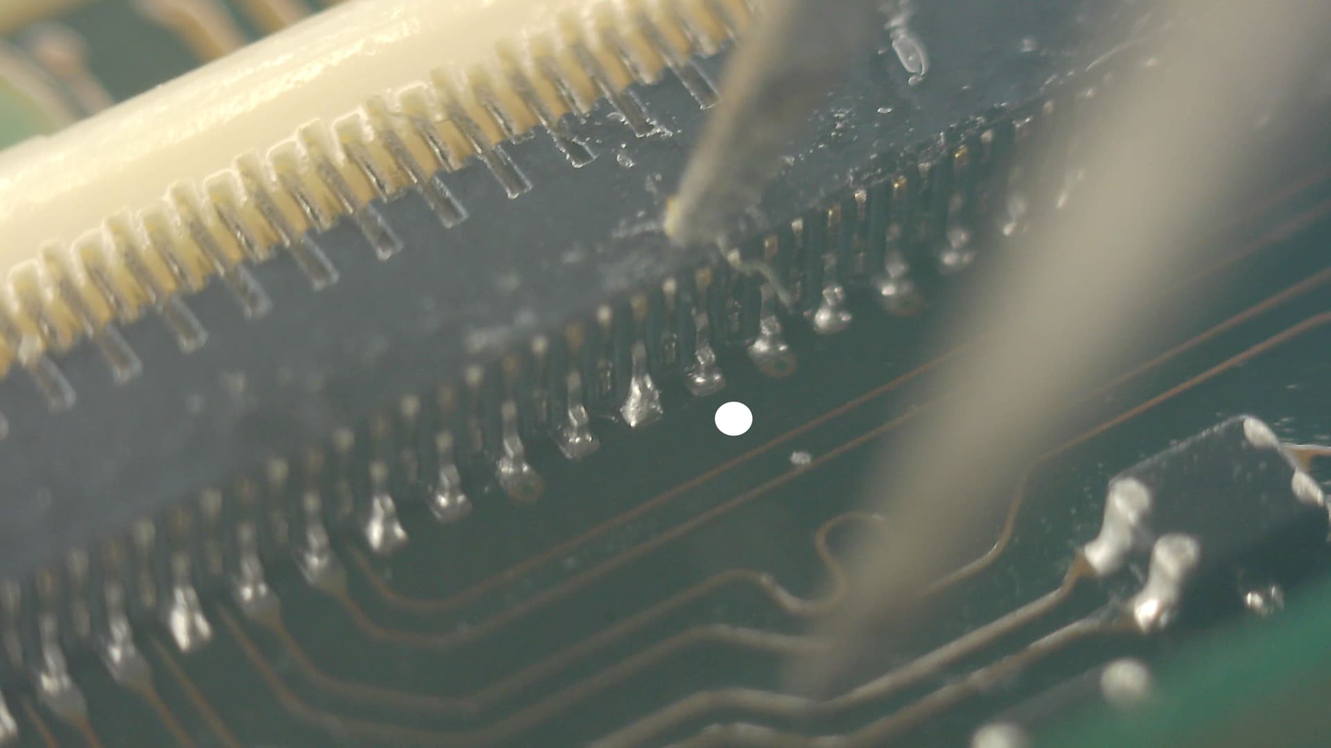
Then I saw, that the LCD connector have bend PINs. I guess I damaged it and now the question is what else I did damage. After replacing the LCD connector I still have a black screen. The backlight goes on but the screen stays black.

I never replaced a connector before, but I guess I managed to put it on decent enough.

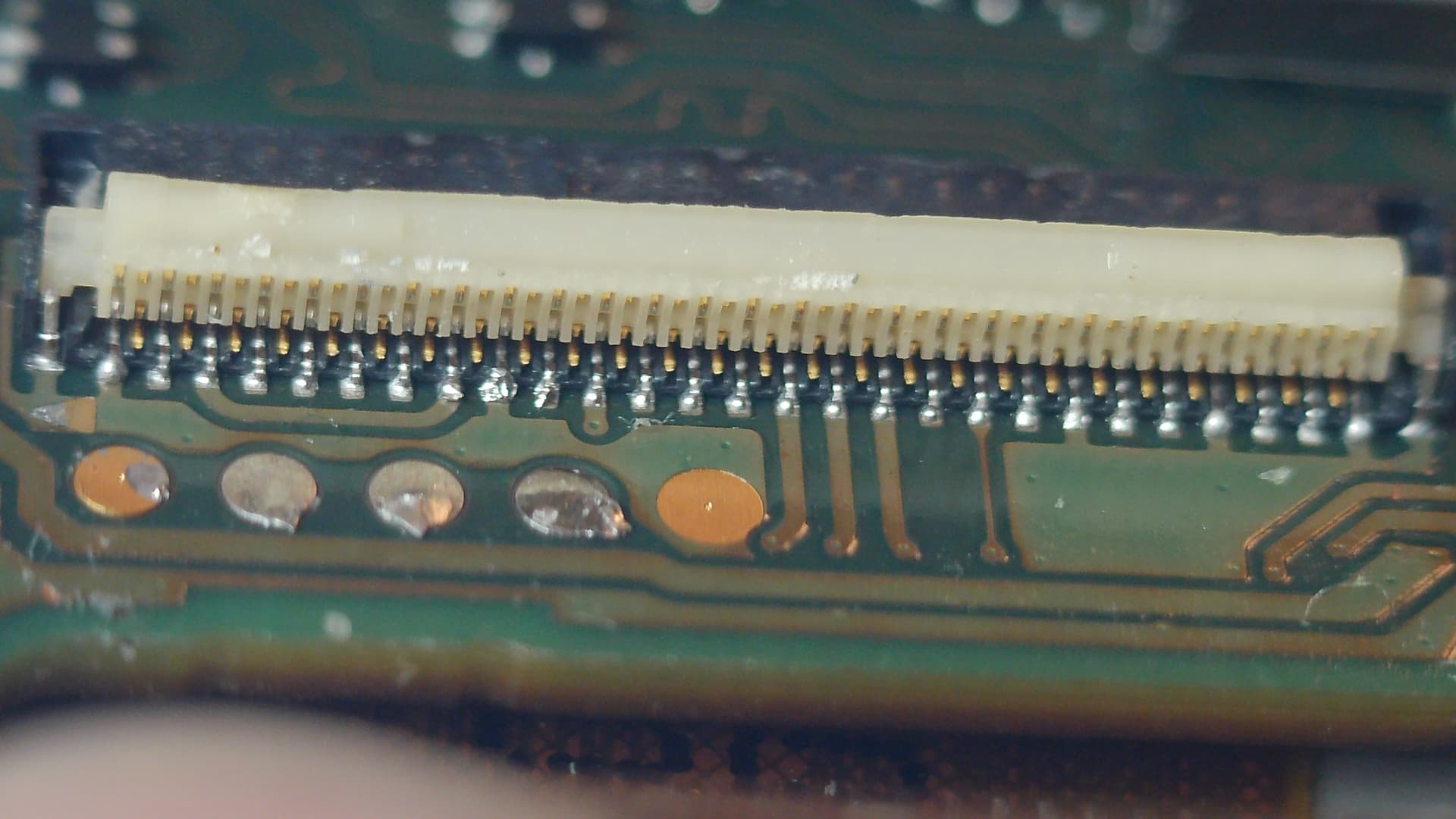
This is the new connector. The back looks good:

The front is only okayish:


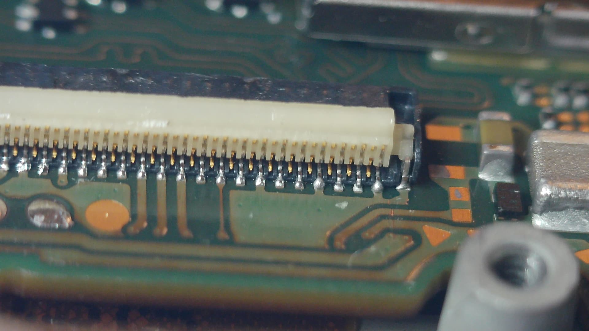
But I guess the connector isn’t the problem?!?

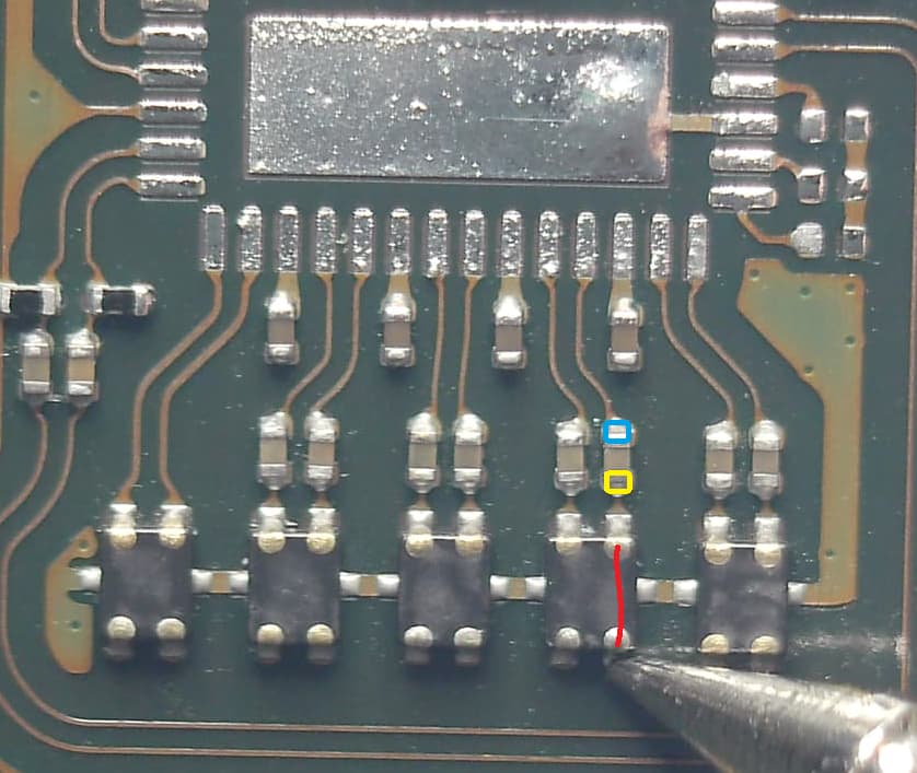
I found various topics in this forum about the 8316 and this picture:

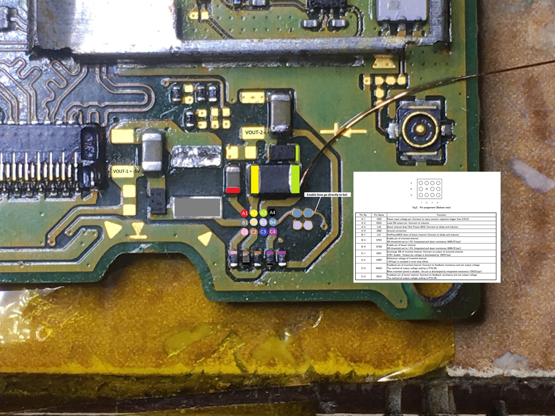
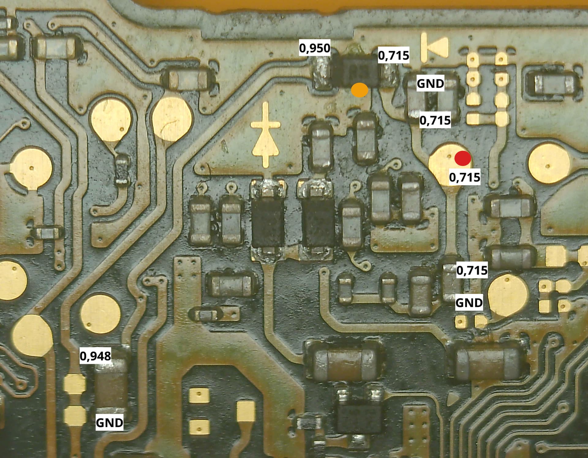
VOUT-1 and VOUT-2 are +0.022 and +0.156V in my case.

The “enable lines” have 1.8V and the A1 connected capacitor got 4V. I also unplugged the battery and measured 358 Ohm on VOUT-1 and 7.92 kOhm at VOUT-2. I’ve a working Nintendo Switch at hand which measures around 357 Ohm on VOUT-1 and 7.12 kOhm on VOUT-2. Also both show -5.4V at VOUT-1 and +5.4V at VOUT-2. Thus the values seems to be comparable. At A1 the working Switch has 3.7V.

So I don’t know how to process further. What does 0V on both VOUT really mean? Is the 8316 broken?

Any help would be much appreciated.

Hmm, another finding is strange.
Before I opend up the switch, I used my USB-C tester and did write down the values.

B2, B3, A11, A10, B10, B11, A3 and A2 were all 0L and connected to the filters of P13USB. I checked all the values (in diode mode) with my working Switch and they were more or less the same.

After replacing the P13USB and the LCD connector B2 isn’t 0L anymore but shows a number of 0.001.

Thus I decided to remove the P13USB again to check if there is a short or something. But even after getting P13USB off, the B2 still shows a value and is not 0L.

It is this filter, B2 is connected on the probe side, B3 on the left of the probe:

The filter itself seems to be okay. Continuity mode beeps only on the straight lines.

Everything else looks okay around P13USB:

I also checked all the PINs within the USB-Connector. They are all good, so no bend pins inside.

But I don’t know if this issue is related to the LCD issue or not.

I assume that your 0 in diode mode is a propper short to ground. I would remove the filter and check again at the usb c port side, if the short is gone.

Simple logic, the cap in between TX/RX choke filter/cut out DC voltage, so if you have short/low diode reading on “blue label”, you have PCB layer issue.
If short/low diode reading on “yellow label” side, check your usb port if pin mango inside or remove the filter and see if it was the filter internal short

Hi,

thank you both for your efforts helping me. I’m really sad but I guess I found the problem with the B2 ↔ filter short to ground. First I removed the filter but the short was still present. I even then removed the LCD connector again. Measuring continuity between B2 and ground did beep. Then I thought I’ll test with another USB-C tester because I have two of them. And the second one showed 0L and did not shorted to ground. I then checked it with the working Switch and the first USB-C tester shorted there too. Testing the USB-C tester outside the Switch does not beep but as soon as I put it in either Switch it short. Thus I guess that was a false alarm. I’m really sorry that this wasted your time. :frowning:

But the original problem is still present. No output in handheld mode. No +/-5V on VOUT-1 and VOUT-2. Do you have any idea what to check next? Should I remove the diode near VOUT-1 and check the diode outside?

I purchased an OLED where the connector was replaced and looked fine. I checked pin by pin to make sure the connector was making a solid connection with the board and checked that there weren’t any bent pins in the connector. In the end I replaced the connector and the screen started working. With all of that being said, I would first check cable display cable itself, clean it with IPA and if it looks fine then I would replace the connector again. I heat the board from the bottom to flow the connector in place.

Hi JuanC,

thank you very much for your help. Yes, I was also not sure if the ribbon cable might be a issue. Thus after your post I decided to disassemble the working switch completely. I then connected the working switch with the display / ribbon cable from the non-working switch. The display worked fine with the working switch. Thus it is not the cable nor the display.

I watched a lot of videos about reparing the switch and found a really helpful one. They measured the board via diode mode and also showed some points for the power rails.

I’m in the process of measuring it via diode mode. Thus I measured around the 8316 and found this:

Diode mode measurings working switch:

Diode mode measurings broken switch:

Thus the cap facing the 8316 chip shows the value of 0.725 but shows OL for everything else.

The golden pad which is marked with a red dot is connected to the back of the board to the golden pad (also marked with a red dot). There the measurements are:

working switch:

broken switch:

So even the 0.948 value on the big cap on the left side doesen’t have a value on the broken switch.

I don’t know if the problem is on the bottom or on the top of the board. I also measured the component with a orange dot. I assume this is a smd diode. If I put the black probe on the left and the red one on the right then I get 0.245 V on both Nindendo Switches. If I switch the probes then I get the OL. Thus the diode on the bottom should be okay.

On the top it is harder to test the diode. Thus I choose another measurement point:

The red probe on the left side of the cap and the black probe on the golden pad shows a value of 0.140 V on the working switch and OL if I switch the probes. And the same measurement on the broken switch shows on the same points OL. But I don’t know if this is a valid measurement because it is not directly on the diode.

Before I remove this presumed diode, I wanted to ask for advice, because its a really tiny component surrounded with the other components. Is my assumption correct that this is a diode and that it seams that it is broken? Do anyone know what kind of diode I need to buy to replace it?

Or do you think my measuring method is not correct because the issue could be on another place and I should check something else?


Check your connector pins, I dont think you have it seat well

Hi jkyoho,

thank you for your help. I had a look on the connector and measured every pin / pad. I did this with the working switch and the broken one and compared the values. I found 4 pins which have OL instead of a value:

Front:
Instead of 0.713v I got OL on both wihte marked pins:


Back:
On this pin instead of 0.913v I got OL


On this pin instead of 0.713v I got OL

All the pins with missing 0.713v are connected to the cap near the 8316:


I used the continuity mode and put one probe on top of the connector and the pin and the other probe on the cap. Thus I didn’t just measured the pad but the pin. Because the pins have a connection to the cap near the 8316 IC I would assume that the pins have a solid connection to the PCB.
I couldn’t find the connection from the pin with the missing 0.913v near the 8316. I guess this is connected to the back of the PCB because is has a hole and on my last post I was wondering about the missing 0.948v on the big cap. Maybe they are connected somehow.

the 4th pin with OL goes to the cap you having OL instead of 0.715 and it also goes to the backside the red dot you label. I assume you have the LCD connector removed by heating from bottom side.
If you still have continuity from the red dot from back to the front side, you might have issue on 8316. Otherwise last time I seen such weird issue was caused by backside layer overcooked

Yes, the red dot on the bottom and the top of the PCB do have continutiy. Also the pin on the back of the LCD connector which should have 0.913v ist connected to the back. I get continuity on the big cap on the back of the PCB which should have 0.948v. Thus the connection between the top layer and the bottom layer of the PCB seems to be working.

I removed the LCD connector by heating from the bottom and it took a while. Thus I also thought that maybe something got damaged on the bottom side. But I dunno if the missing handheld mode is due to a short I produced while the connector had bend pins or if I destroyed something on the bottom side.

Because I got the Switch with a working handheld mode and broken TV mode and now it’s vice versa…

Okay, so then I’ve to order a 8316 from china because there is no 8316 in my country. Do you think the diode near the 8316 is also dead? Because on the working Switch I get 0.140v and OL on the broken one.

I decided to remove both diodes near the 8316 and both are showing OL in diode mode no matter which direction I put the probes.

I would guess that this shouldn’t be the case?!?

Do anyone know the magic words to find such diodes? The picture says 8 A, but searching for diodes and Nintendo Switch only shows a diode near the fan connector with the name ‘71’.

Or can I use another ‘standard’ diode?

At the V1 boards this two Schottky Barrier Diodes at the lcd power ciruit are from On Semi: NSR05F40NXT5G

Hi Calvin,
thank you very much for providing the part number. I found the parts. Before I order them I decided to take them from my working Nintendo Switch because they are not that cheap in my country (with delivery fee it will cost around 10 bucks / €).

And I can confirm that after using both working diods from my working Nintendo Switch the broken one now is working again. Thus it was the diodes. I have now the values at the back of the PCB. The Nintendo Switch is working in handheld mode as well as in docking mode.

Thus thank you all very much for helping me again to solve this issue. This one was really hard and took a few weeks and a lot of work and also effort from you guys. Without you I wouldn’t be able to find it.

I will now order the diodes and put it into the doner (working) Switch to get it working there again.

One more thing. Both Nintendo Switches were open for several weeks. I guess I should replace the thermal paste. But it is not a regular one like for CPUs. Do you have a suggestion what to use?

I don’t think that the thermal paste is effected by been opened for some weeks. Beside dust or fingerprints. I usually use MX4 to apply new thermal paste if needed.