Right, these are identical, check the datasheets, the company either merged or was bought out by another company
As for whether the chips have to come from a donor, are fused or have a specific FW, well the genral consensus has been stick with chips from donors… but I don’t recall ever trying a new IC myself and just took other peoples word on this…so perhaps this one is a myth
You may want to search the forum as I made a post a while back detailing where you can check BT/WF enable lines as well as info verifying the antenna (and some support circuitry which directly attaches to the antenna)
Also, if you could clean the general area (think good enough to eat off) and inspect the chip on edge and ensure you can see good connection on all sides and after provide a photo just incase anything jumps out which may not be obvious
My switch lite have no wifi,and I found that even when I removed the wifi chip, my switch still worked fine, it does not stuck on any logo,all functions are normal except that there is no wifi and Bluetooth, the system does not report any fault code. The game can also be played normally. Some people have had the same problem?
Haha, sorry. Yeah, it’s very dirty… what would you use to clean the flux residue? I am always struggling with that (with IPA and cotton swabs). Preferably without the need for an ultrasonic cleaner
I will check all the accessible lines and report back. Thank you so much!
By the way, wouldn’t a fault in the support circuitry render both bt and wifi not working? They seem to both be using the same antennas.
I typically batch all my boards up and stick em all in the ultrasonic in a row when I’m done. If it’s a localised area where it’s not worth sticking in the ultrasonic then you’ve got a few options. Load up a cotton swab with IPA and also flood the area on the board (I like to use a syringe for my IPA with one of those tubes like what you get with WD40 pressed onto the syringe) then with your hot air at… I don’t know… let’s say 140 to 180C medium to high air, heat the area while swabbing around the IC and general area and resaturate your swab and the general board area as you go, the IPA and heat will wick out the spent flux and the swab will sap it up. Trouble with this method is you;ll burn through IPA quick but it works, keep doing this until it’s clean…
You can also introduce 30% deionized/distilled water into your IPA also which will lessen how quick it evaporates and tends to do a better job of disolving spent flux and as a side affect it also lessens that white residue which IPA often leaves behind (though in truth this residue has little to do with the IPA itself but rather the contaminents still left on the board) just make sure if your using distilled/deionized or a mix that the board afterwards is fully dry before connecting power/turning on, while neither would cause any damage if left wet, strange things can happen if left wet due to minute impurities, especially in HF RF circuits such as this (that being said I’ve observed similar things with 99% IPA so it’s not really a huge issue)
In general the antennas are the same, but if you trace them back they have their own independant support circuitry on the board, namely each haveing some unknown component each (a small 6-pin IC) … RF stuff boggles the mind and is outside my wheelhouse… maybe opamps
I don’t think so… I think the IC/s in question a more likely to be the diplexers, but as I haven’t positively identified these components/got a datasheet for them (or even tried tbh) I’d sooner say I don’t know. The RF switchers would likely be prior to the Antenna>Diplexer>RF Switch>BCM as per the application circuit
I hope not just for my sake, or in the hopes that it will somehow fix your board it was just so when you take a few photos of the general area I can get a better idea of what’s going on and see if there’s anything off, chences are that I probably won’t be able to spot anything
btw I think there was a topic here on the forum at some point relating to ultrasonic cleaners which I posted on detailing some of the common pitfalls and mistakes people make when buying and using them so you may want to see if you can find that, for example, seeminlgy legitamate companies selling a rebadged glass cleaner as a “PCB cleaning solution” which it absolutely is not and cause serious issues to boards
Actually I have quite a few pieces of repaired tech that would benefit from a PCB cleaning. Mostly GPUs. I’ve been teaching myself how to repair stuff in the last half a year as a hobby. It’s pretty fun and as long as the profits cover the losses+equipment costs (which it does for now) I am fine
And, while this bluetooth problem seems to be rather puzzling, it’s a good opportunity to learn new stuff. So thank you again so much for all the advice and pointers.
One thig which I may not have touched on relating to ultrasonic cleaniers in the other topic, which is quite important, which I’ll just cover here. You’ll be tempted to ultrasonic boards more than you ought to at the begining ie: either for too long, or at to high a temperature or just multiple times, you’ll learn pretty quickly not to do this, for a few reasons. A legit ultrasonic solution is corrosive, it has to be, this is how it does it’s job but continual cleanings or too long etc will ultimately result in components effectively being eaten away, this shows itself most obviously on passive component endcaps, if you keep going you’lll deterioate them or you’ll be inadvetantly trimming resistors and the like. The other issue with going too far with the ultrasonic is moisture, even though the dilute (with deinozed/distilled water) is perfectly safe for electronics, the presence of liquid can linger, even after drying the boards in an oven (which I’d reccomend you do after ultrasonic following an IPA rinse) this moisture gets trapped between board layers and if it’s not sufficiently dry, then come rework time that moisture has to go somewhere during evaporation and typically it’s going to take the path of least resistance and often it will be in the form of board popcorning which fundamently writes off the entire PCB, so be careful
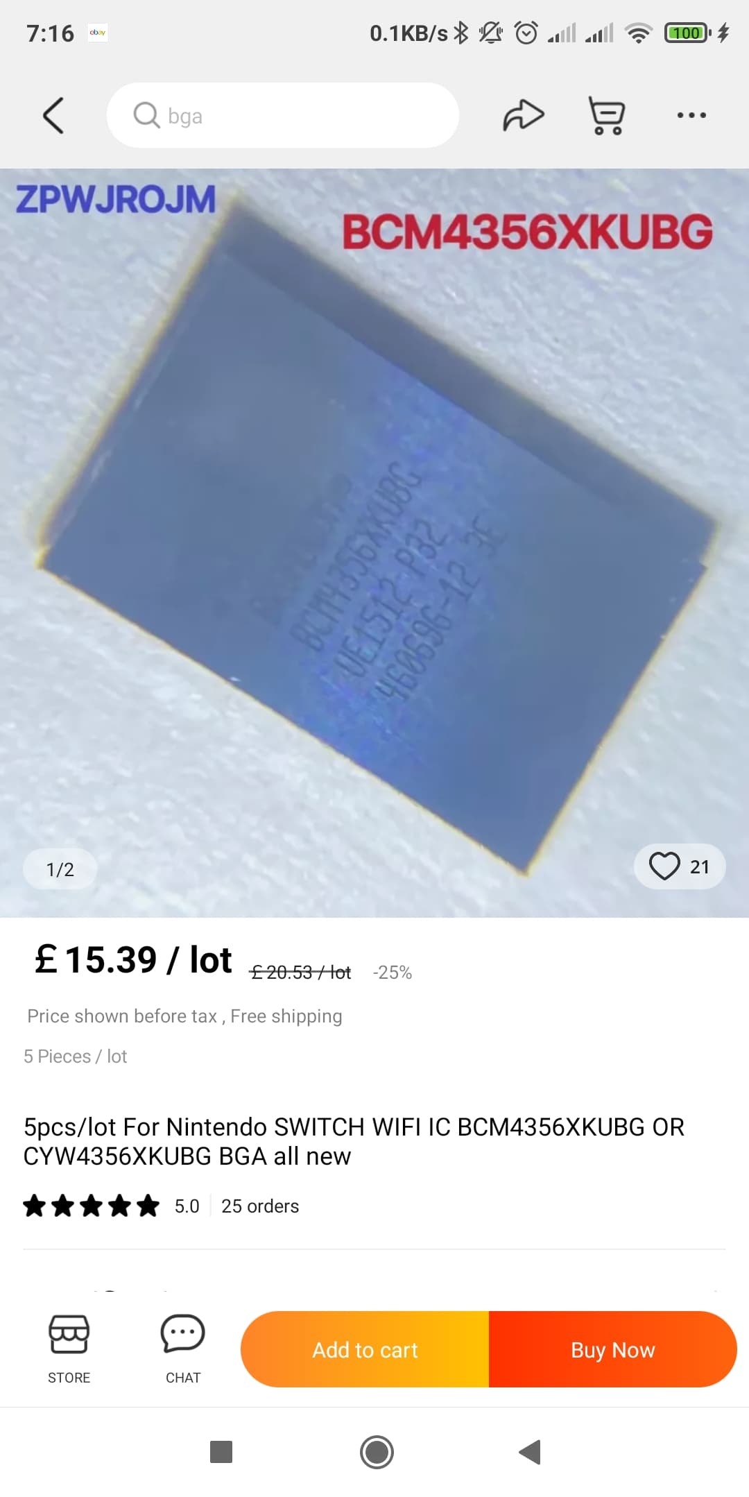
in my experience, these chips get WiFi but no Bluetooth. (not new like the listing suggest) one looked new the rest didn’t. but I reballed them all anyway.
I had a total of 5 switchs I did this weekend. (mostly V2s.
I installed the chip from this seller. (I ordered the cym ones but they sent the broadcom ones.
when installing these chips I failed to get Bluetooth. so I pulled the WiFi chips off other PCBs I have (didn’t check which version. and both Bluetooth and WiFi worked fine first time
I repeated this 5 times in a row pretty much and got the same results. so I don’t personally believe it’s my method. as everytime reballed one I pulled off a board myself it always works on the same switch I had problems with these chips.

 Thank you so much!
 it was just so when you take a few photos of the general area I can get a better idea of what’s going on and see if there’s anything off, chences are that I probably won’t be able to spot anything