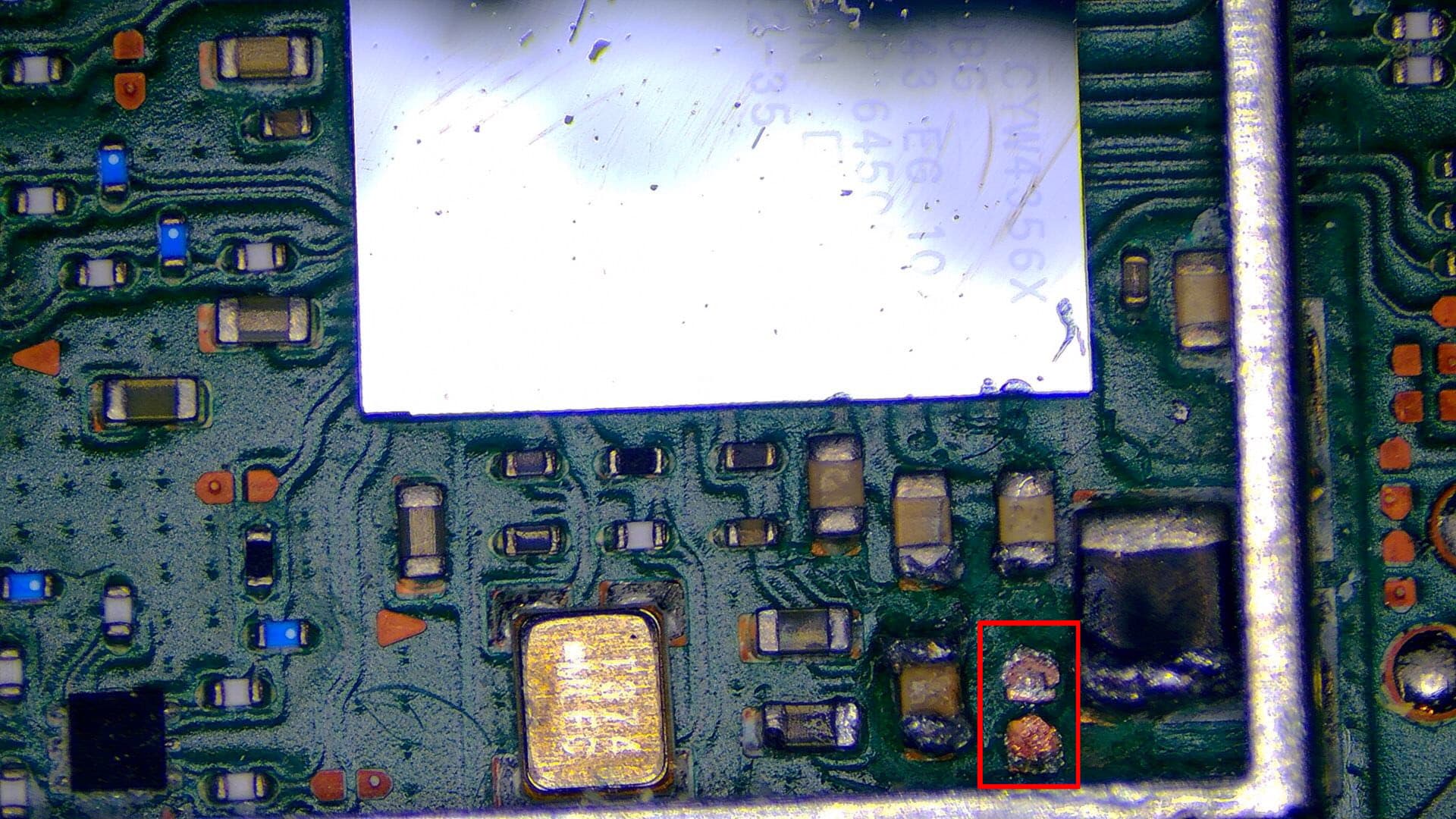
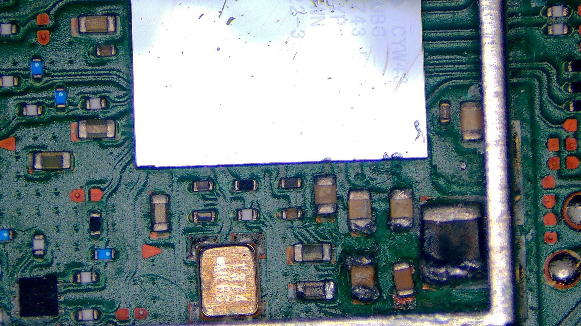
I managed to knock a cap off near the wifi/bluetooth IC while cleaning some corrosion underneath the shield.
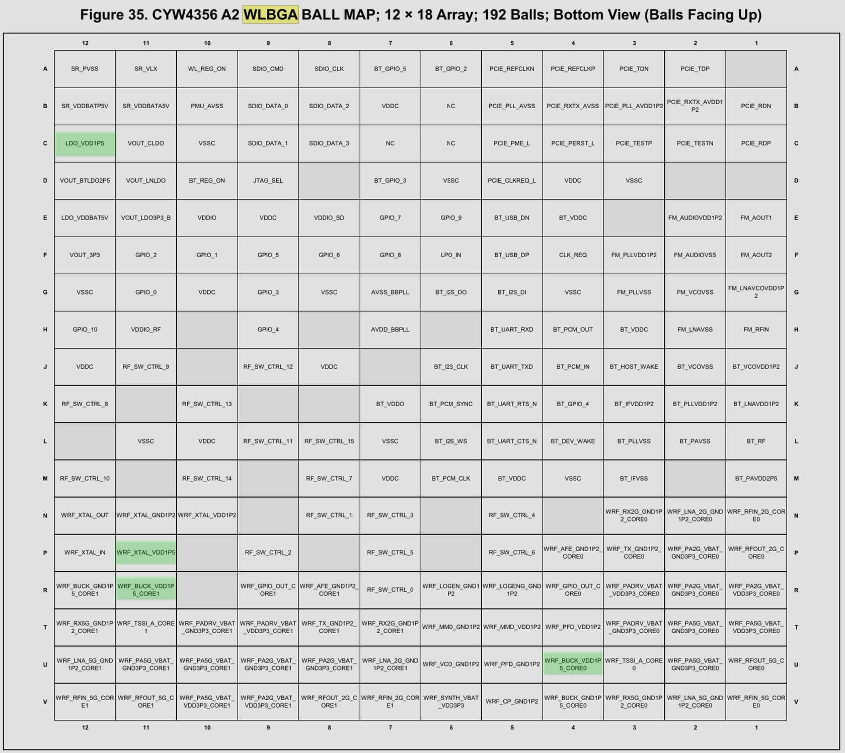
I’ve checked the datasheet for the CYW4356 to check the relevant pad information:
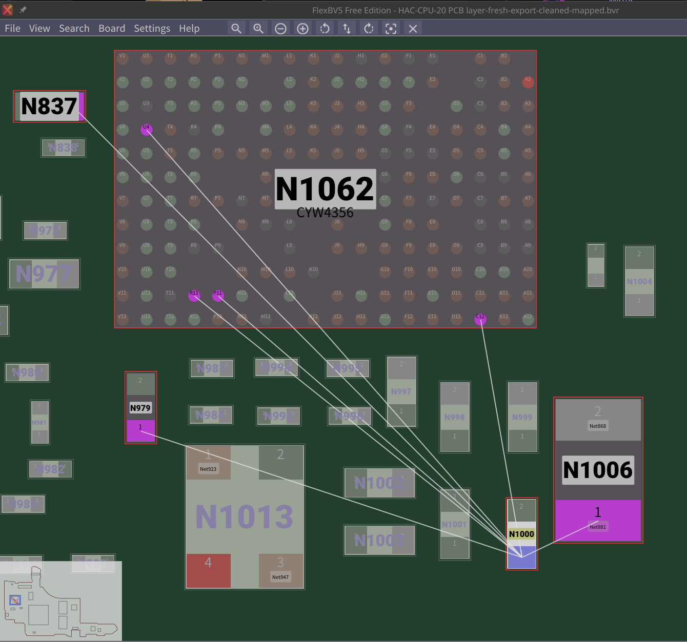
U4 and
R11 : WRF_BUCK_VDD1P5_CORE0 and 1 are apparently for an ‘internal capacitor-less LDO supply’
P11 : WRF_XTAL_VDD1P5 is an XTAL LDO input (1.35V)
C12 : LDO_VDD1P5 is an ‘LNLDO input’…
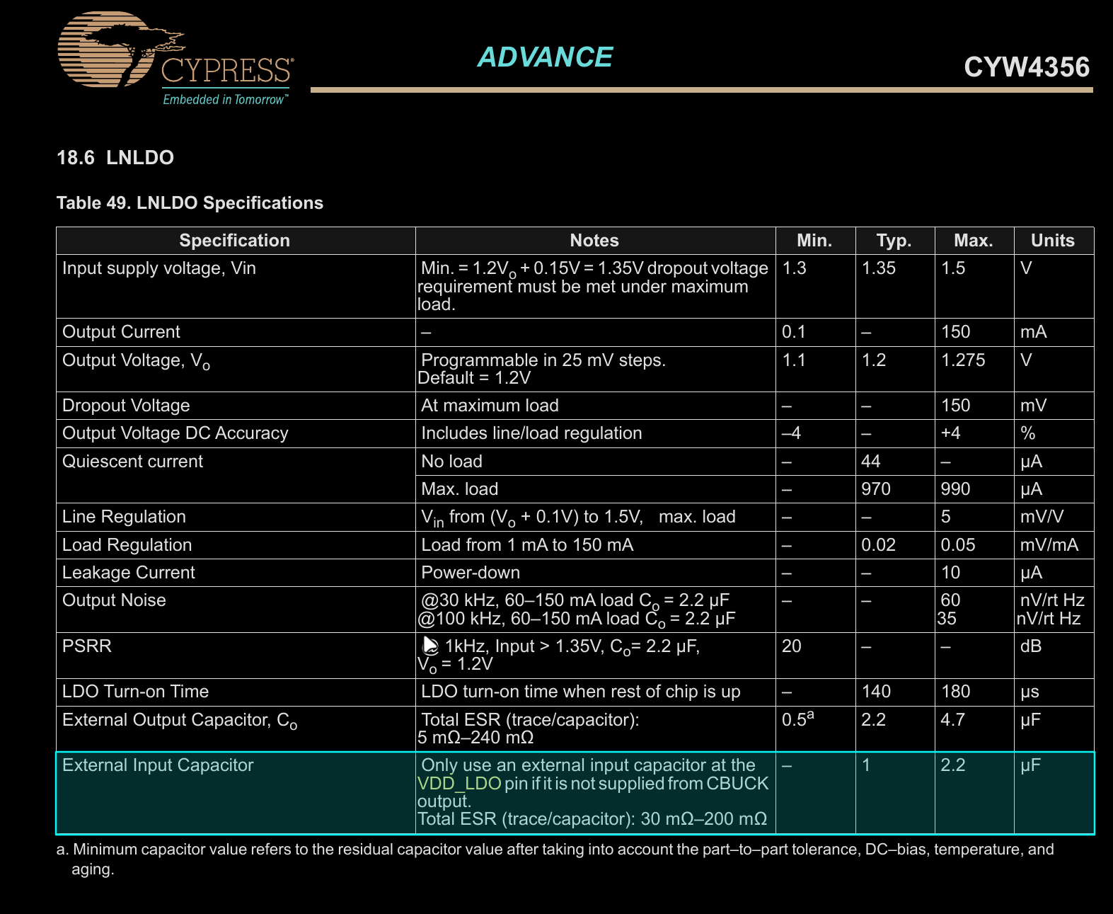
Am I following that correctly, and that should be a 1µF or up to a 2.2µF cap?
This is a 1uF 0402 10v cap in the space, seems smaller than the others, slightly, so it’s possible it’s actually the 0603 4.7 uF cap, (it does appear to be next to an inductor, which the CBUCK regulator has?)
Looking more closely at the traces, I’m fairly certain this is the external output capacitor for the internal CBUCK regulator in the CYW4356, that is being shared to serve as input for the LNLDO (pin C12:LDO_VDD1P5)
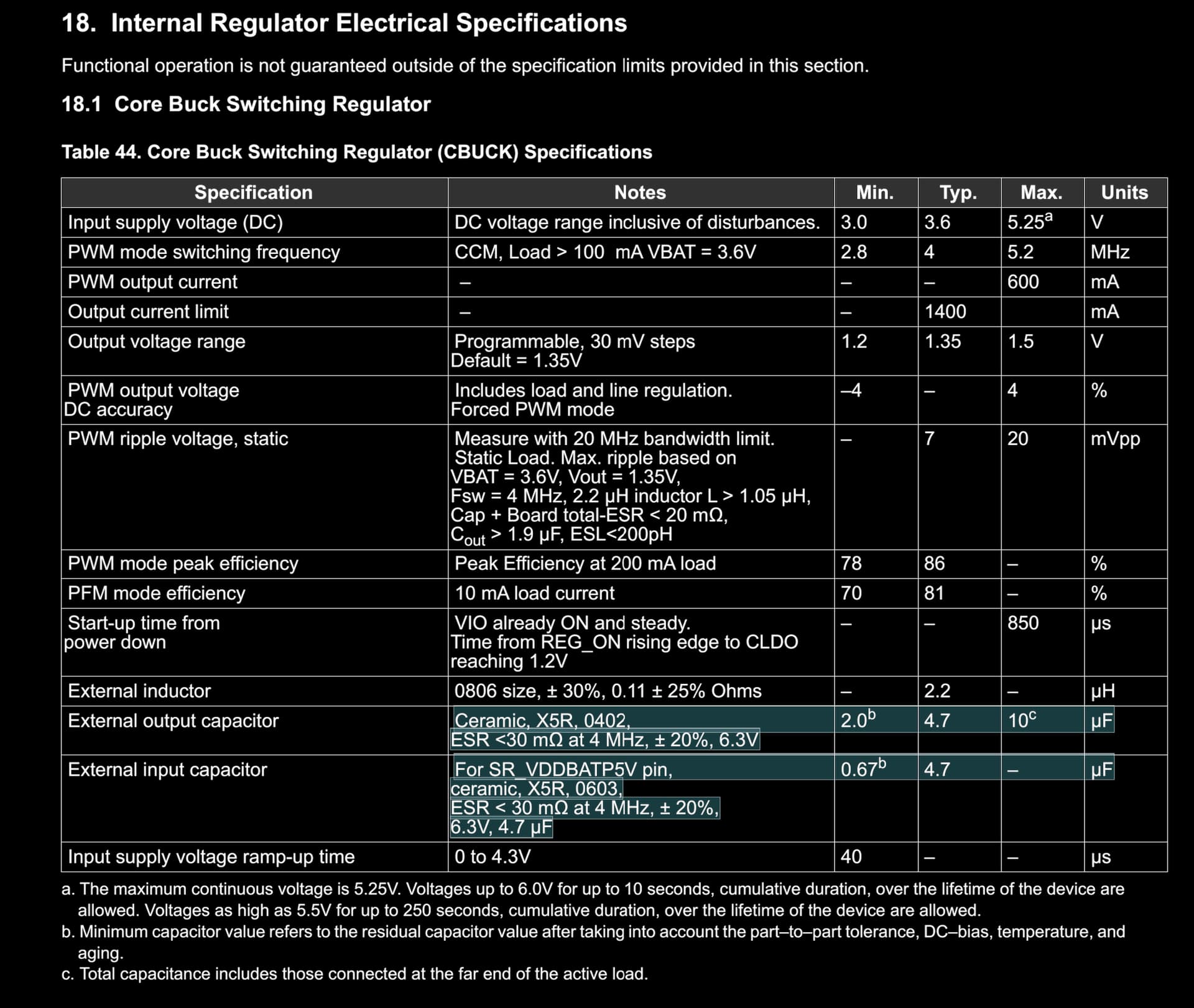
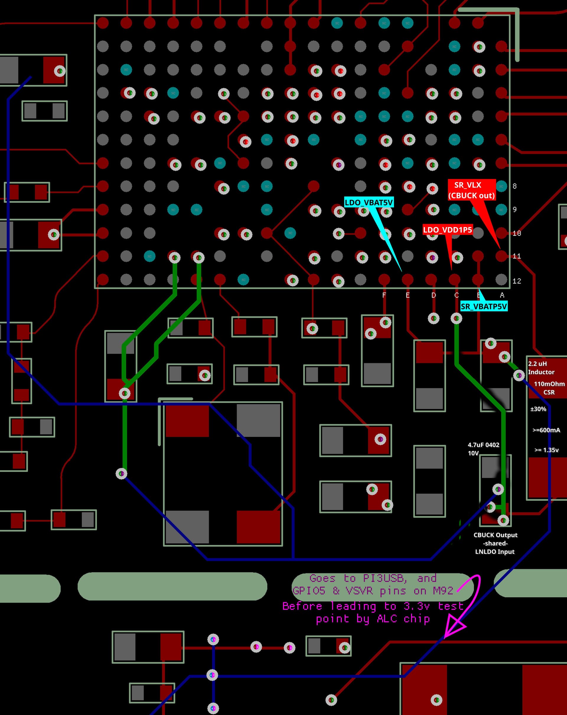
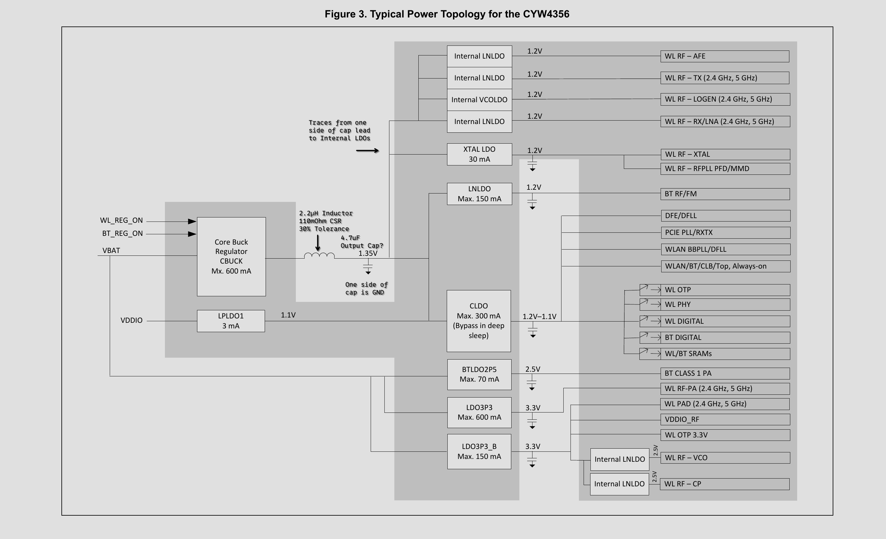
Pin A11 is labeled SR_VLX, and the output of “Cbuck switching regulator output” referred to in Table 44 (uploaded in the last post). It comes down through a 2.2uH, 110mOhm CSR, inductor, before moving to a 4.7uF 0402 capacitor with one side grounded, and the other on a Via that leads to the 1.35v input of the “WRF_XTAL_VDD1P5” and “WRF_BUCK_VDD_1P5”.
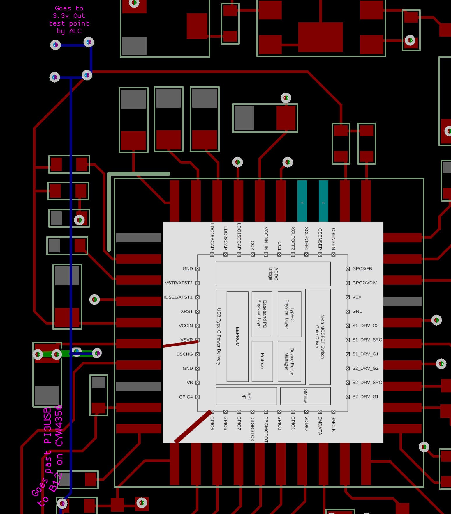
Pin B12 is labeled SR_VBAT5V and is labeled an input. this trace goes past the PI3USB, to the M92’s VSVR & GPIO5 pins (5v rail?)
This all seems to line up with what Figure 3 shows.
I apologize for the messy or overly annotated images… I had originally thought that maybe the top capacitor was a directly related input/output, and that finding out what the connected pins were for might help me to understand… It turned out to be a completely unnecessary ‘research’ endeavour, other than maybe explaining how the chip gets its power from VBAT.
Thought I’d share this info here in case it helps anyone else. Also, on the off chance someone sees something glaringly wrong with this, please do let me know, I would appreciate it.