Upon attempting to install a PicoFly modchip on a Switch Lite, I ended up damaging the left DAT0 pad. Are there any traces I can follow, or alternate points?
[Reposted due to incorrect tag]
Upon attempting to install a PicoFly modchip on a Switch Lite, I ended up damaging the left DAT0 pad. Are there any traces I can follow, or alternate points?
[Reposted due to incorrect tag]
Can this pad being missing prevent the console from powering on? And also, is it possible to remove the metal shielding around the chip? (Not the top part)
Yes, it will stop console boot up.
You can remove the metal if you want
Thanks for the reply. What is the best way to remove it?
Ask yourself why your removing it or want to remove it? given the cause of damage to begin with i think it might be a bad idea for you to go down this path… ripping it off and potentially damaging the board (further), or two inadvertently messing up the EMMC install (or other) by using hot air in the area to remove it, or three using low melt solder and potentially contaminating the area… again, what is the purpose/reason for you wanting to remove it?
Given what Jkyoho has said above I imagine the TP is a via which is why he’s saying it won’t boot without it (though I haven’t looked at the board scans myself to confirm) - so as he said, you have to dig down with a blade and find the VIA nub and reattach and connect to the any other line it would ordinarily connect to, you shouldn’t have to remove anything to accomplish this. All I’d say is if your a beginner this might not be the time to practice and if you know someone with a bit more experience or there is a decent repair shop nearby it may be better to have them do it ![]()
I think I may have already scraped too far and destroyed the via. The area where the pad was is just black.
Womp womp.
I’ll probably just check to see if anyone would be willing to try and fix it properly and install the chip. Or just use the console as a donor.
This is my first time working on a Switch, and definitely the most difficult modchip I’ve ever attempted. I don’t have a microscope either. Rather, I was using my phone’s camera to magnify the points.
Can you post a picture of the area?
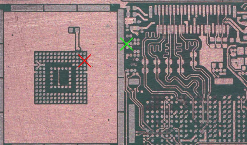
This is what it looks like. Just quickly opened it back up.
htt/ps://imgur.com/a/DjvmAZY
(I can’t post links on here, so just remove the slash at the beginning.)
Bit hard to tell bud from that image (dunno, you might wanna see if you can get a cleaner shot of this just so i can confirm), would imagine the copper I think i can see round the edge in that little crater you’ve made is ground? the via nub should be directly in the center provided you haven’t already burned through it at it’s destination layer , if you have might be worth checking those board scans as you might be able to pick up the trace by exposing a small section of the ground plane above… though all the warnings i mentioned above apply as this is a pretty complex job for someone new to this, so if you plan on having someone else work on this might be best to just leave it alone and make their life a bit easier ![]()
ps: hopefully you haven’t been using a rotary tool to do this and don’t plan on doing so (?)
Unfortunately, it doesn’t seem fixable. I think I might have already gone through that layer while scraping away at it.
I’ll see about getting a replacement motherboard and using this one to mess around with.
Thanks for trying to help though. Until then, what size tips are best for working on Switch consoles (T18 tips)? I was using a chisel tip and then tried a bent tip, but I’m thinking of getting a 1.2mm chisel.
Where are you located bud? I could fix this for you if in the same country
Really depends on what work your doing, I’m usually using a chisel D12 or D24 for most things but in cases like yours where your having to tin a via nub in a crater you’d probably want to use a J type tip, but if your tip isn’t the best quality or your station isn’t up to it (and because this style of tip has such low thermal mass) you may have to have your hot air help out at approx 100/140C while using it.
Often what happens is, flux starts to burn before the nub properly tins (due to the low tip mass and likely poor contact) and then starts to look almost like treacle making it seem like the via is lost…so might be worth heating the area up at about 150C with hot air (to soften the flux) and IPA and toothbrush while your doing that, clean rinse and repeat and hopefully you’ll see the VIA nubs copper appear.
I think next on your purchase list is a optical trinocular microscope (don’t waste your time with digital) that will make your life so much easier ![]()
I’m located in West Midlands, UK.
And yep, I agree that a microscope would be a good thing to buy considering how finnicky digital ones are, let alone using my phone suspended by a boom arm. And of course the next thing being to learn how to stop ripping solder pads off PCBs.
I recently bought a bent tip for my FX888-D and I like it a lot. It’ll be useful for small spaces like that. Although I’d also like to get a small chisel. I also use SRA 63/37 lead and MG Chemicals rosin flux, along with 99% IPA.
Oh, I’m not far off, I’ll send you a DM if you want ?
Was this using a ribbon or enamel wire? if enamel wire, sometimes when the gauge is too thick it can put undue stress on the pad and can quite easily pull off. If ribbon, that’s a bit of a mystery ![]() In both cases, pads which have a VIA below are usually pretty tough because of the “anchoring” so you’d have to try pretty hard to pull them off or perhaps soldering iron too hot (?) did you lose it while soldering or?
In both cases, pads which have a VIA below are usually pretty tough because of the “anchoring” so you’d have to try pretty hard to pull them off or perhaps soldering iron too hot (?) did you lose it while soldering or?
There is a blade style tip I have which is thinner than the regular K type style, I’ve forgot the name but I’ll have a look, it’s thin enough to get into tight areas but is wider so has quite a good amount of thermal mass.
All good choices ![]()
The pad came off while I was trying to solder a ribbon wire (30 AWG) onto the two DAT0 pads. The station was set to 325C at the time. As I struggled to try and solder the wire because of it being such a tight space, I realised that the pad was gone. I tried to scrape away at the area but just ended up making a huge crater. I don’t think any of the other pads are damaged however. I also ended up breaking off the interconnect cable clamp next to the battery, but I’d be willing to live with that as long as I can secure it in some way.
It might just be better for me to get another board and try it again, or have somebody with more experience install the Picofly for me. Unless you would be willing to give it a shot?
Are there any microscopes you could recommend? Ones that are not prohibitively expensive but work well?
I see, unusual at such a low temp
Hey I could take a look and hopefully condcut the repair and install and update this thread with what I’ve done which may be helpful to others but - just as a heads up it’s won’t be free ![]() If your interested I can send you a PM but maybe you wanna hold this off and save this board later for yourself when you’ve gained some more experience and gotten a microscope
If your interested I can send you a PM but maybe you wanna hold this off and save this board later for yourself when you’ve gained some more experience and gotten a microscope ![]()
pretty much all the trinocular scopes on the market are the same and any that appear different are just a rebadge, so opt for the cheapest on Aliexpress or other. Avoid the binocular scopes (Switft/amscope style with non standard lenses) the only thing which diferentiates these are the stands, bog standard sheet steel stands aren’t great but usable, boom arm stands are better but ups the shipping costs
30AWG is too thick for such dat0 pad, since it’s just signal line, you could use 0.1mm enameled wire
Hello, I’m sorry to dig up an old thread, but I’m curious what the final resolution was with this dat0 repair. I have run into a similar issue so I’m hoping that I will be able to recover the console.