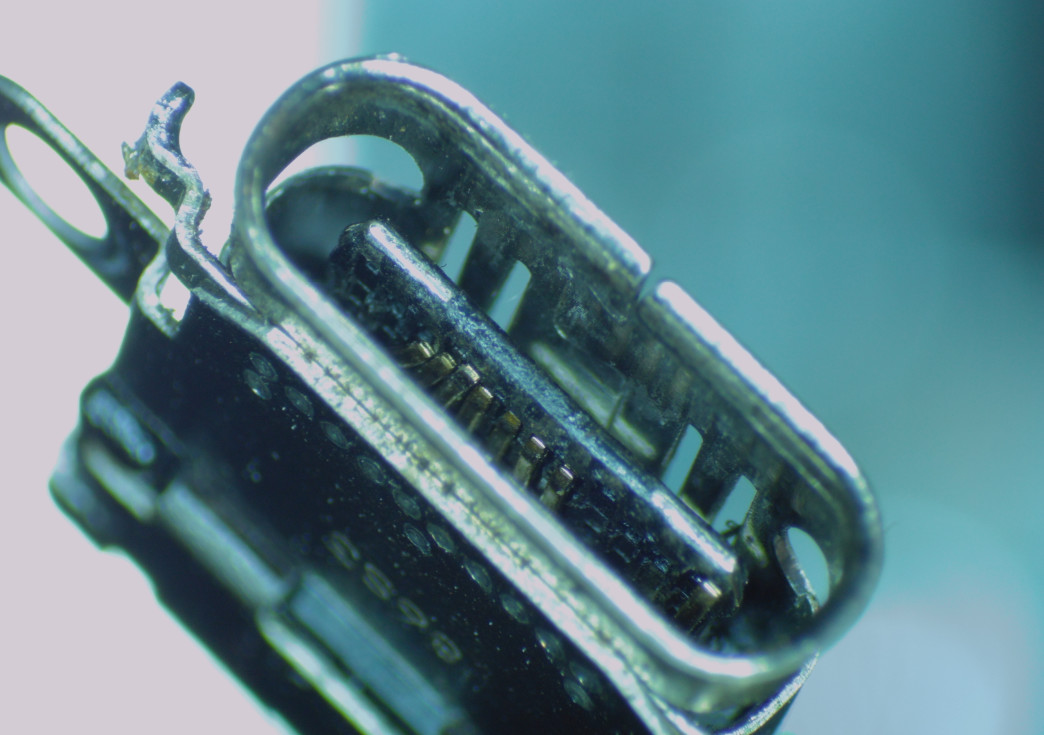
This switch had twisted and shorted USB port pins. No prior rework signs. I removed the USB port and noticed the data line pads are open circuit (all four pads). There were some shorts around M92 which I got rid of by desoldering the IC. Any idea what is causing the data lines to be open? SoC problem?
Where are you measuring between when you say it is open?
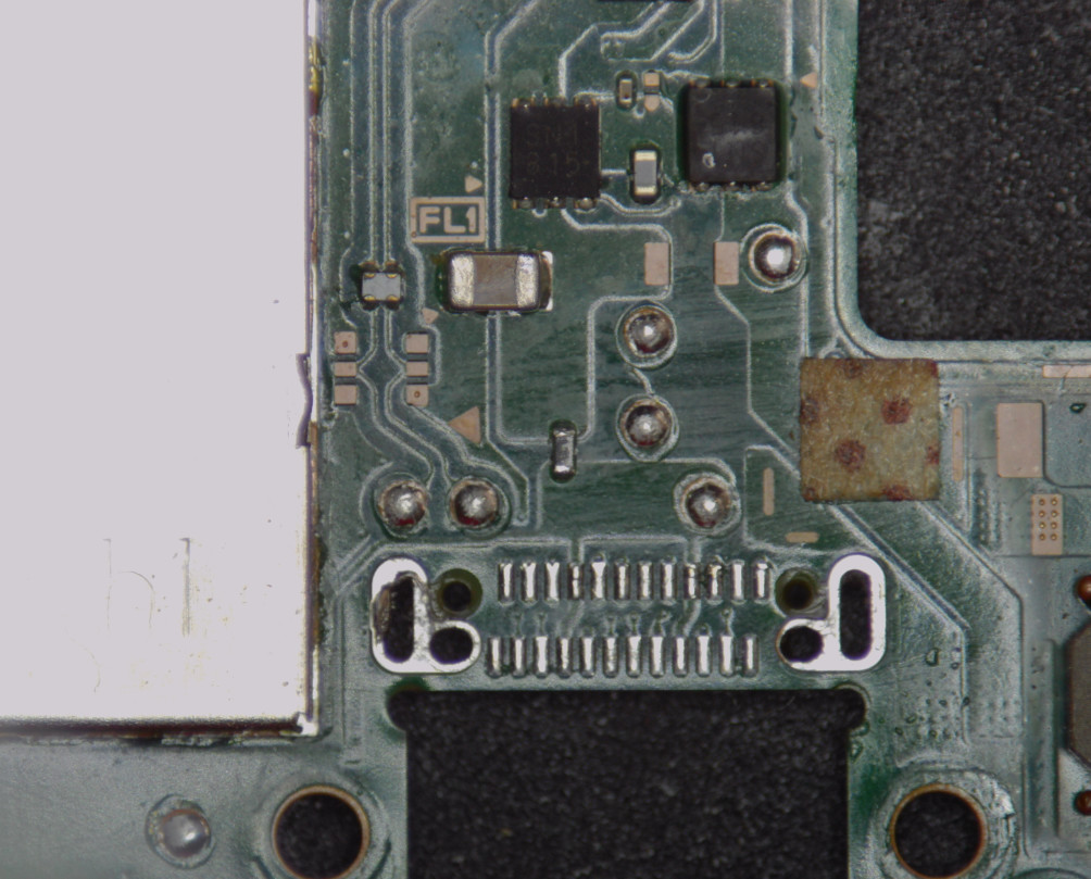
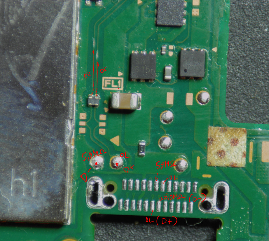
Did you check the filter for continuity (left under the FL1 print) above the D+ D- testpoints?
On the usb port pads, also on two test points next to usb port and the other two test points close to audio chip.
The filter has continuity.
So there is no continuity between the usb pad and the test points just above it? I would be tempted to just run a jumper wire…
Sorry, maybe I didn’t explain the problem clearly. When I mean the line is open, there is no continuity between D+\D- Pads on the test points to ground (resistance and diode mode).
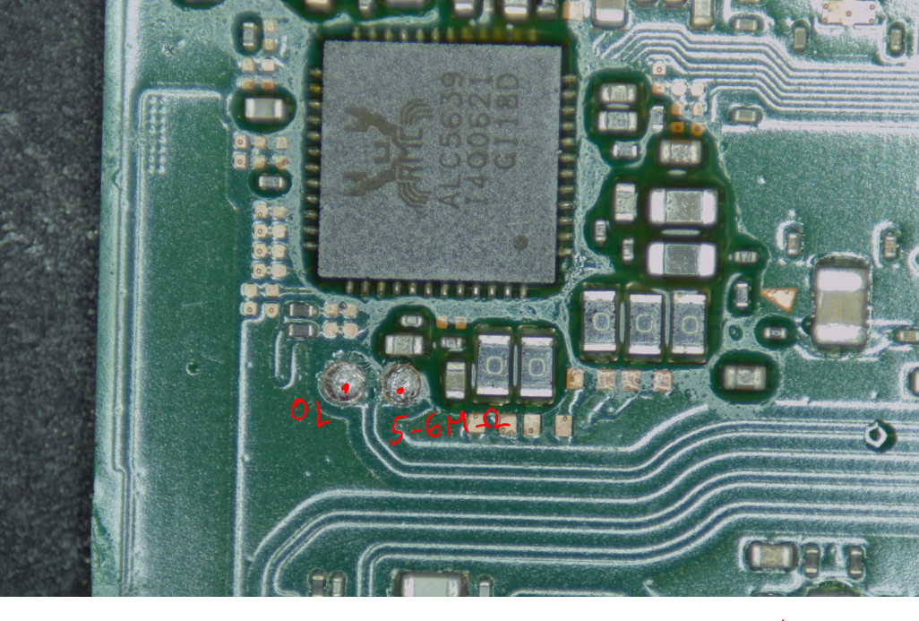
From memory you should have a few megs to ground at these points, and I’m pretty sure they go directly to the SoC this side of the board, so probably indicating an SoC related issue.
It’s also possible your meter doesn’t have the upper range to display these higher values, so it’s worth verifying on a known good to be sure.
What do you get on the opposite side of the board at the TPs out of curiosity?
I’d probably also be inclined to scratch back the traces above that filter and ensure you have continuity, not uncommon for them to fail in a strange manner, where the pins seperate from the package, probing directly across it temp resolves the issue.
1 Like
On a good board I get 0.6M ohms at both test points.
I haven’t tried to power on the board yet. I’d assume that it will boot but not charge.
Was the original cause bent USB pins?
your reading of 5.9M is good the other being OL is not good, likely killed the I/O at the SoC assuming it’s not impact damage causing pad/joint issues.
It’s possible a fault elswhere could cause this but tbh more often than not it’s the SoC
Corresponding balls at the SoC are 2 and 3 row in, pretty much line up with those two caps to the left of the SoC, might be worth have a peak under in that area
Yes, bent and unfortunately pins shorted.
Okay, I’ll take a peek. Btw, I haven’t removed the shield frame around the SoC before. Do I need to use hot air (and protect the SoC)?
To remove the shield I stick a scalpel blade and twist the tabs outward going round all of them, then it just pops off, afterwards you can just squeeze them flat again with flat ground pliers… I notice on a lot of the boards I get in people attempt lift them up and mangle the whole shield in the process.
As for the shield frame itself I tend to avoid removing it as surface tension does not work when putting it back on and it never truly goes back in line, given how terrible the aligment of the copper sticker and plastic (dunno what to call it) ooze prevention (?) sticker is, it might be enough to prevent the copper layer from sticking flat afterwards… hope that makes sense.
If you really do want to remove the frame then I’d go round it with leaded and probably a blade type tip, take multiple passes to saturate it with leaded, if you can find a shield that’s small enough to cover the SoC in the process then yeah, if not you can use a coin over the die, the frame should come off long before the lead free solder melts under the SoC though it still takes quite a bit of heat.
And yeah, given that it was bent pins originally, it’s probably fried the I/O SoC side unfortunately ![]()
I’ll have to look at the USBC spec and see if there is a ghetto way around this problem if the console still boots
1 Like
Thank you for the tips.
I soldered new USB port to check if it charges. Breakout board shows OL (diode mode) to D+/D- as expected. The switch boots normally and charges 15V/0.8A. Didn’t try dock mode yet.
I was in the assumption that both data lines are needed for charging. Seems like it’s not…
Interesting, I would imagine plugging it into a PC would be where the toubles will be as I can’t imagine it communicating without one of the differential pairs. Don’t know about dock
Good read here
Do you measure a voltage on your breakout at D+/-?
PC does not recognize it and the switch says ”unable to charge”
Dock mode and other functions work normally.
D- gives 1.5V when not plugged into charger otherwise OL (or running numbers). D+ gives nothing.
I was lucky with this one. Yay!
That’s great news man, completely usable ![]()
1 Like
Hey there, was wondering if you were able to manage to resolve the issue?
Yep. The USB D+/D- lines are used for signalling using a “phone” charger using USB-A to USB-C cable, so if the SOC I/O is damaged it will never detect and charge properly. However the official Nintendo charger uses the CC lines to determine charging meaning this should still work. Same with the dock.
2 Likes
Yep. I had the same issue with my last one. Replaced port and P13, everything works fine except it only slow charges at 5V and is not recognized by computer. The d+ line was open in my case. A bit of a bummer because the switch had a low serial number thus capable of running CFW.
@SheriffBuck Out of curiosity: I guess reballing the SoC won’t help here because I/O is permanently damaged?