great job,
quick question: how thin was the solder mask, did you heat up from the bottom or the top of the usb port.
great job,
quick question: how thin was the solder mask, did you heat up from the bottom or the top of the usb port.
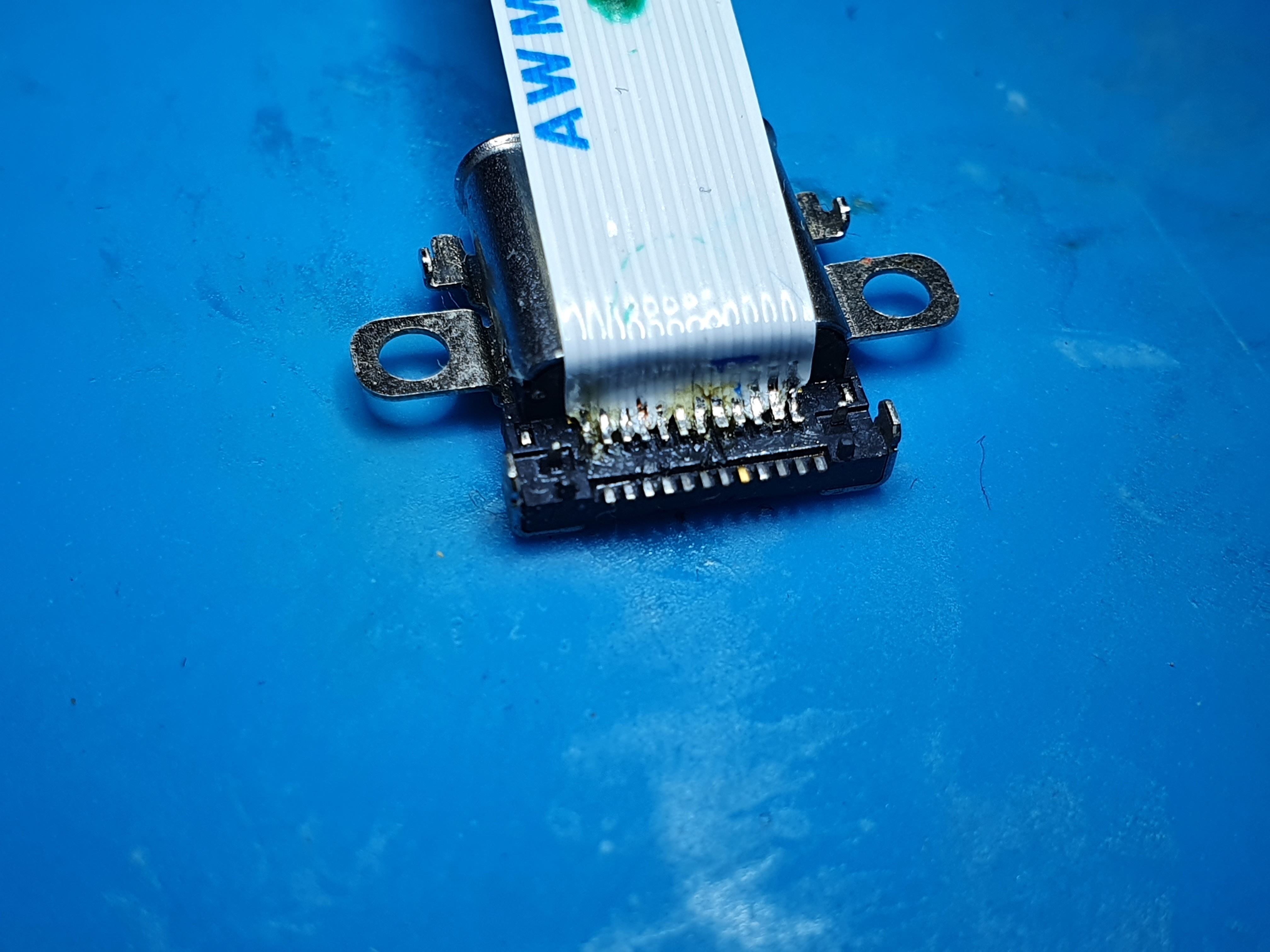
You need to get the solder mask as thin as possible as the connector won’t sit well. You can try to tweak the pins of the connectors down so that they can take up the slack if it makes sense.
I heat from the bottom. It’s a tricky operation as seconds too long, and you melt the inner plastic of the connector, so you need to be quick and ready.
Don’t forget to tin the pads of the connector and the board to maximise bond. And plenty of flux!
how do you clean the initial flux off after soldering the jumper wire? each time I use a q tip it just moves the jumper wire out. Do you tin the jumper wire after the solder mask? Great idea on tweaking the inner rows on pins so that it can try to bond with the jumper wire.
Yep. That’s a pain. So long as you have a good connection, you can afford to disturb the placement whilst you clean. I often use a soft bristle toothbrush and brush in one direction to minimise pressure on the bonds. Once free of flux, you can reset positions ready to apply UV mask to insulate and provide mechanical support. This is an important stage as not getting all flux off well compromise the bond of the mask.
REFOX Soldering Lug For Pads Repair

I am actually using this now. I’ll report back if I am successful.
When using UV mask, cover the pad with mask and after putting the UV lamp 2-3 minutes with a spatula, clean the hardening mask from the surface you want free for tining. It will work without fail.
(www. you tube. com/watch?v=NUR54Wo0JRI)
I did my recovery this way, I recorded the procedure, it worked perfectly!
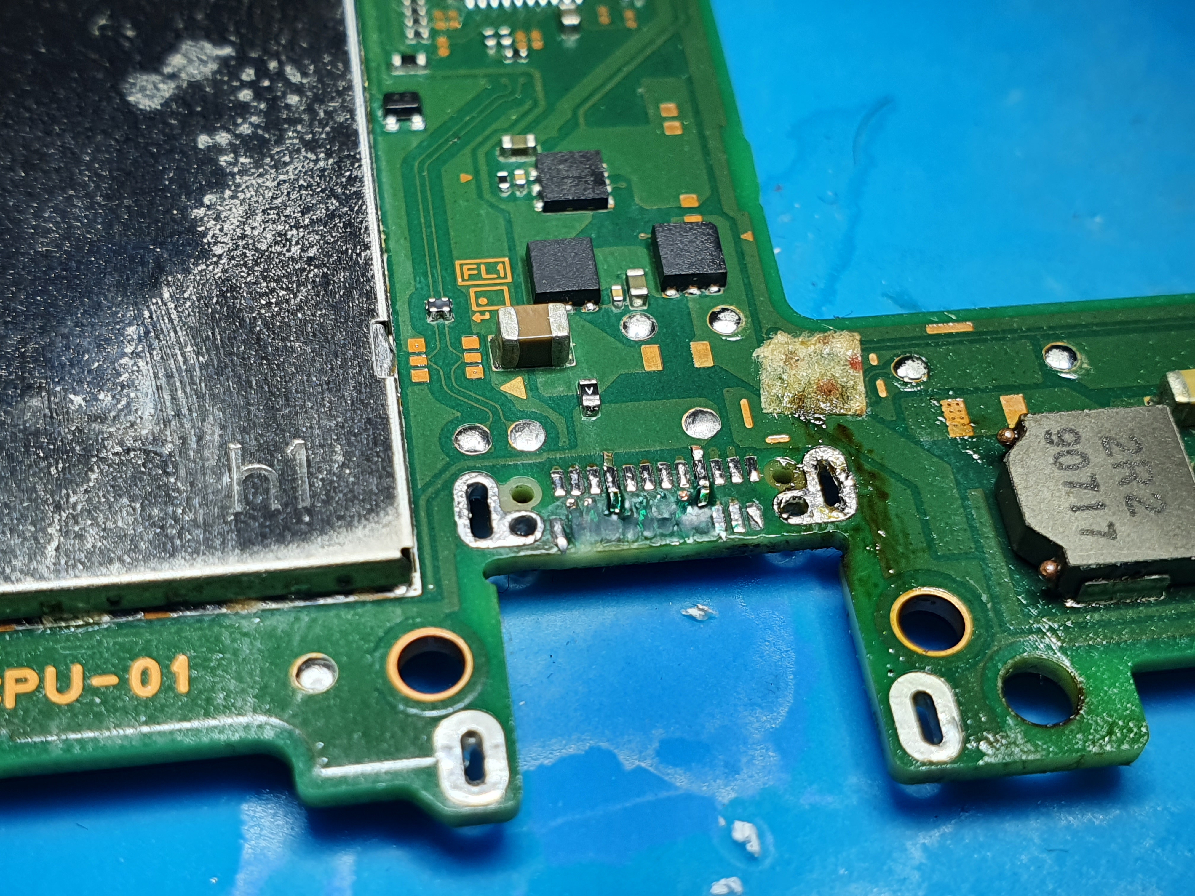
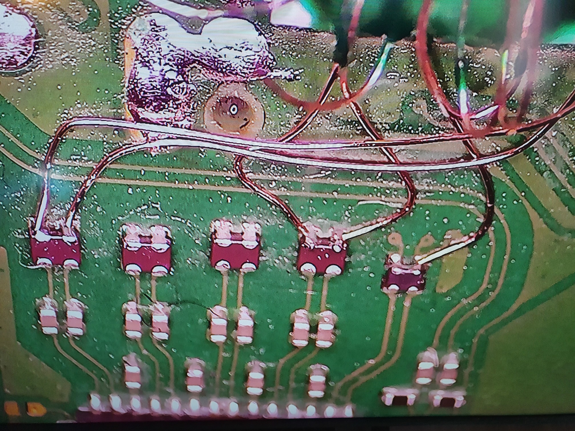
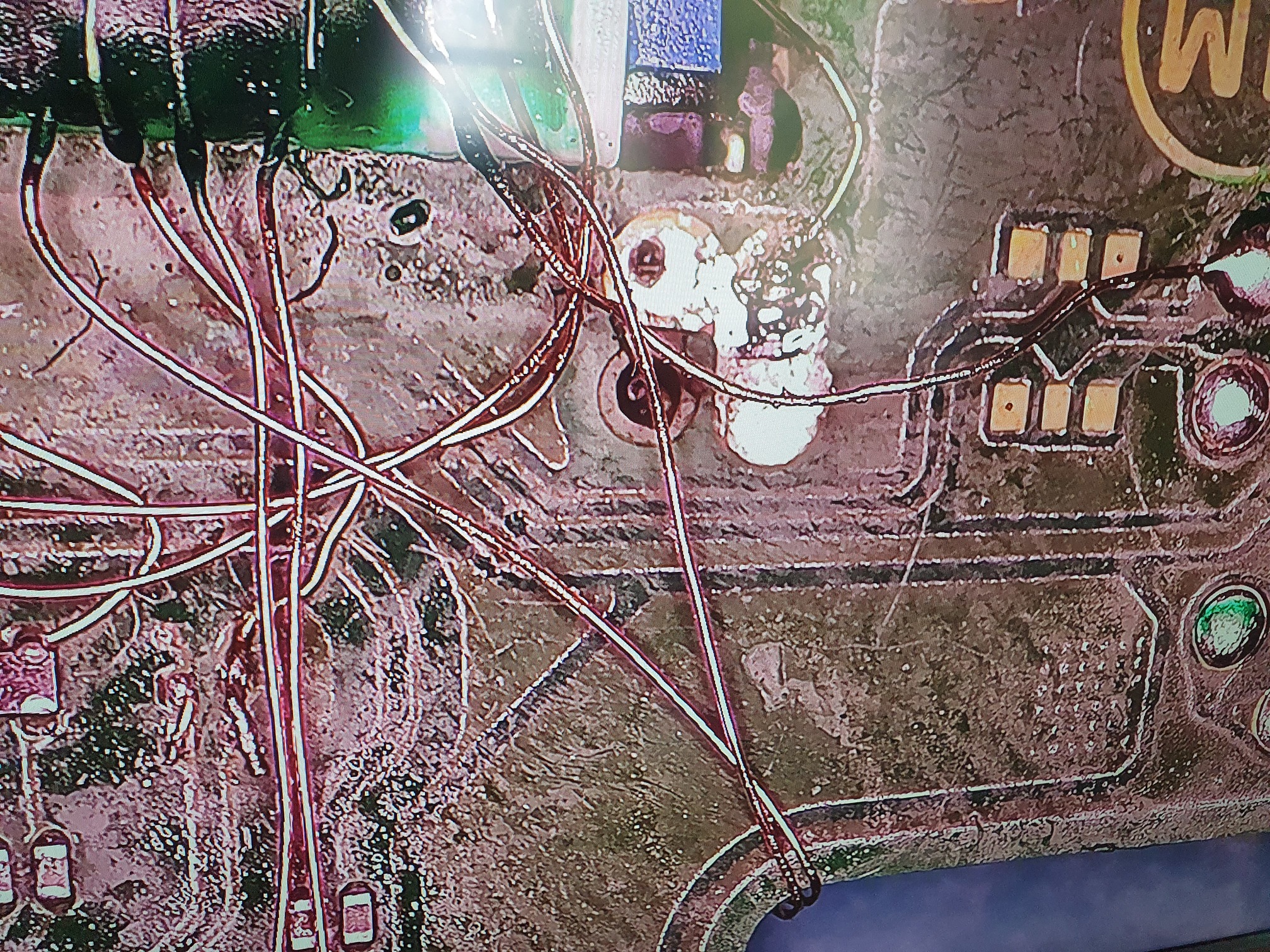
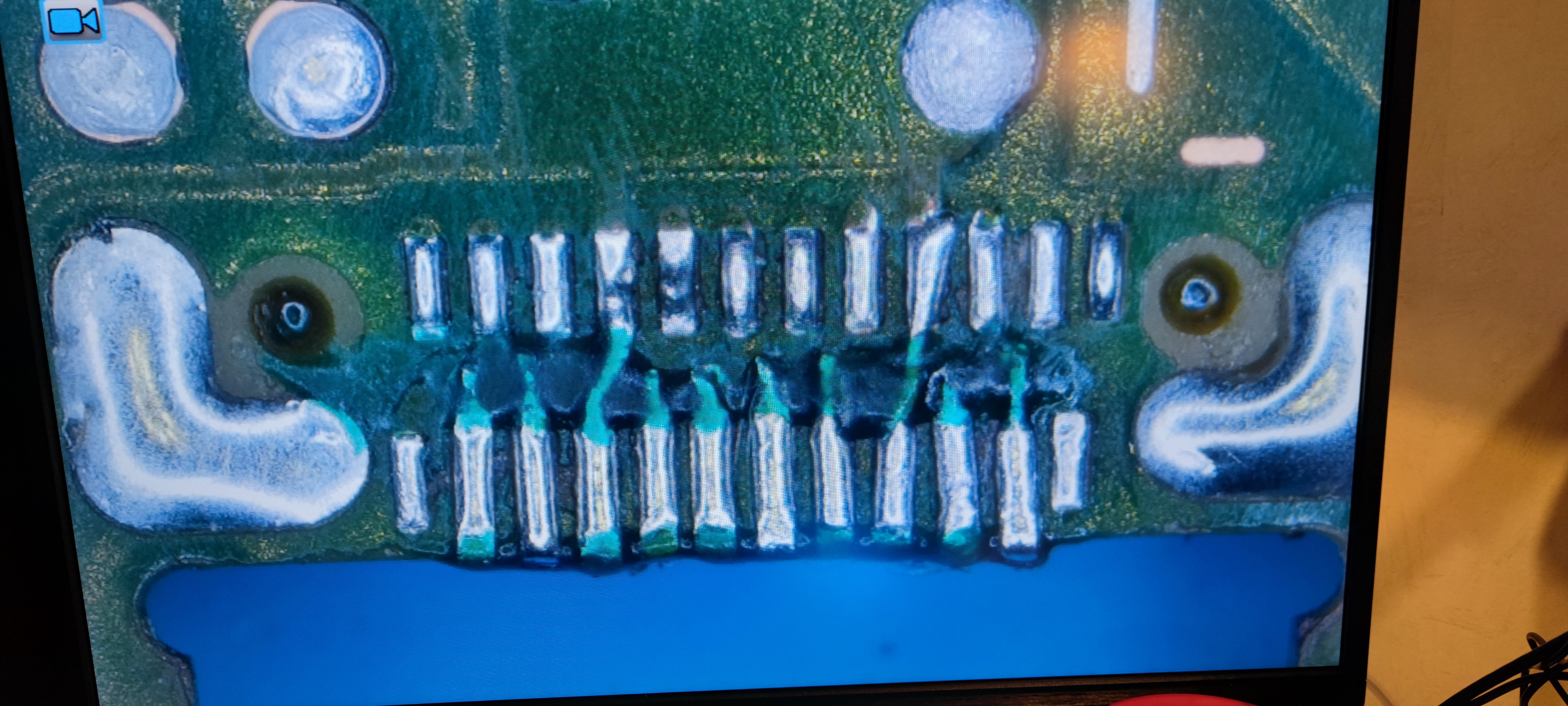
Hi there. I want to thank you for creating this thread and also share my experience that I had with attempting to fix this problem. I got a Nintendo Switch the USB port of which had badly bent pins and it wouldn’t dock anymore, but charge. I wanted to replace the USB port and of course, it was my first time, I destroyed some pads. After I found that too many pads were completely ripped out and not being sure which pad has which trace directly adjacent to itself, I decided to go with “method two”  i took me actually months to get all the parts and tools together, mainly because of delayed shipments. I ordererd solder mask, 0.1 mm isolated jumper wire and ribbon flex cables (those are exactly ones you can find in a PS4 controller, with 12 connectors, 0.5 mm each), and some good quality tweezers.
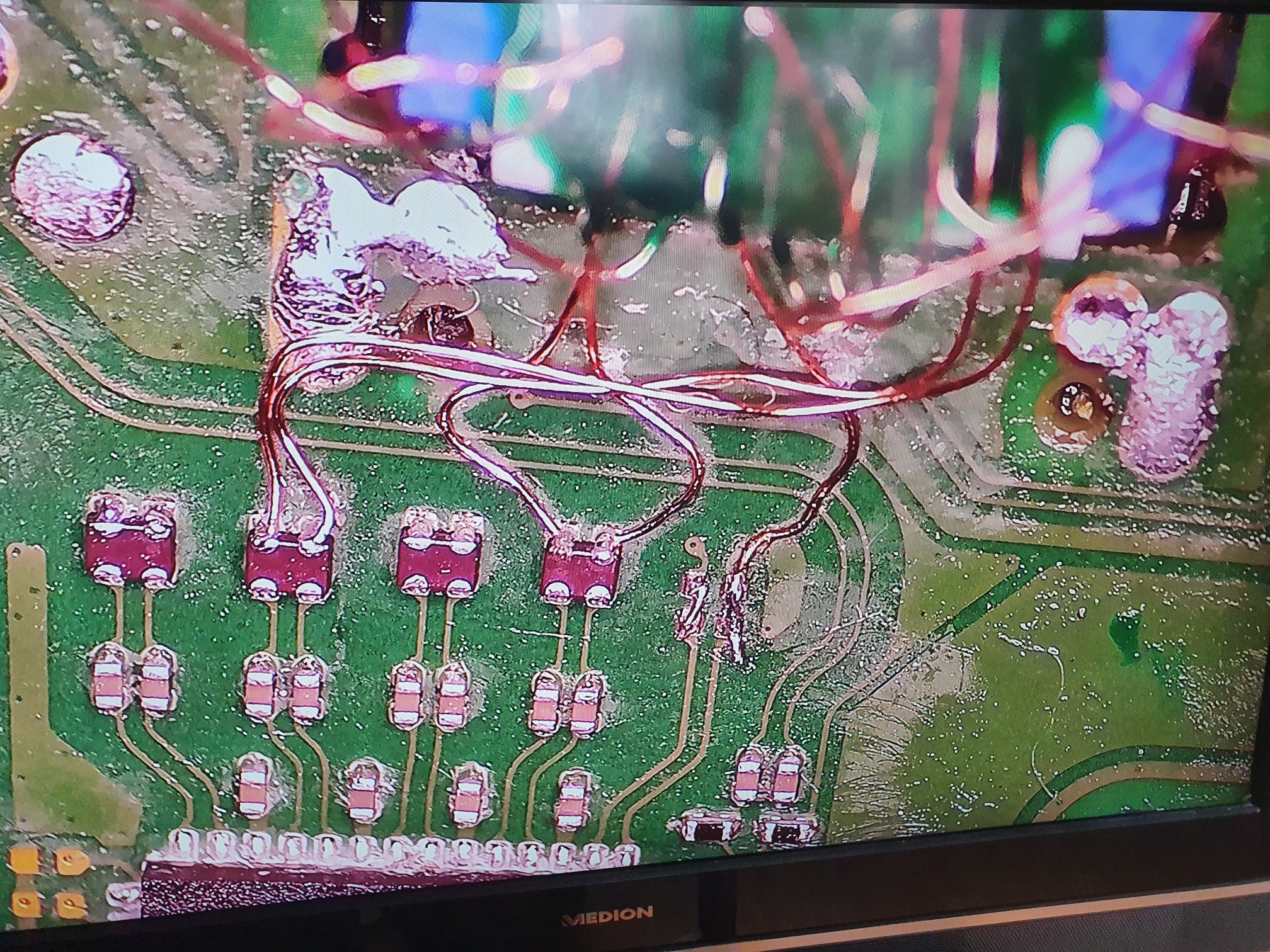
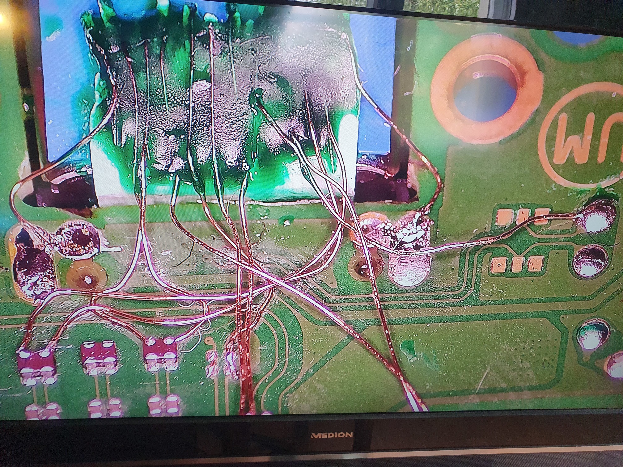
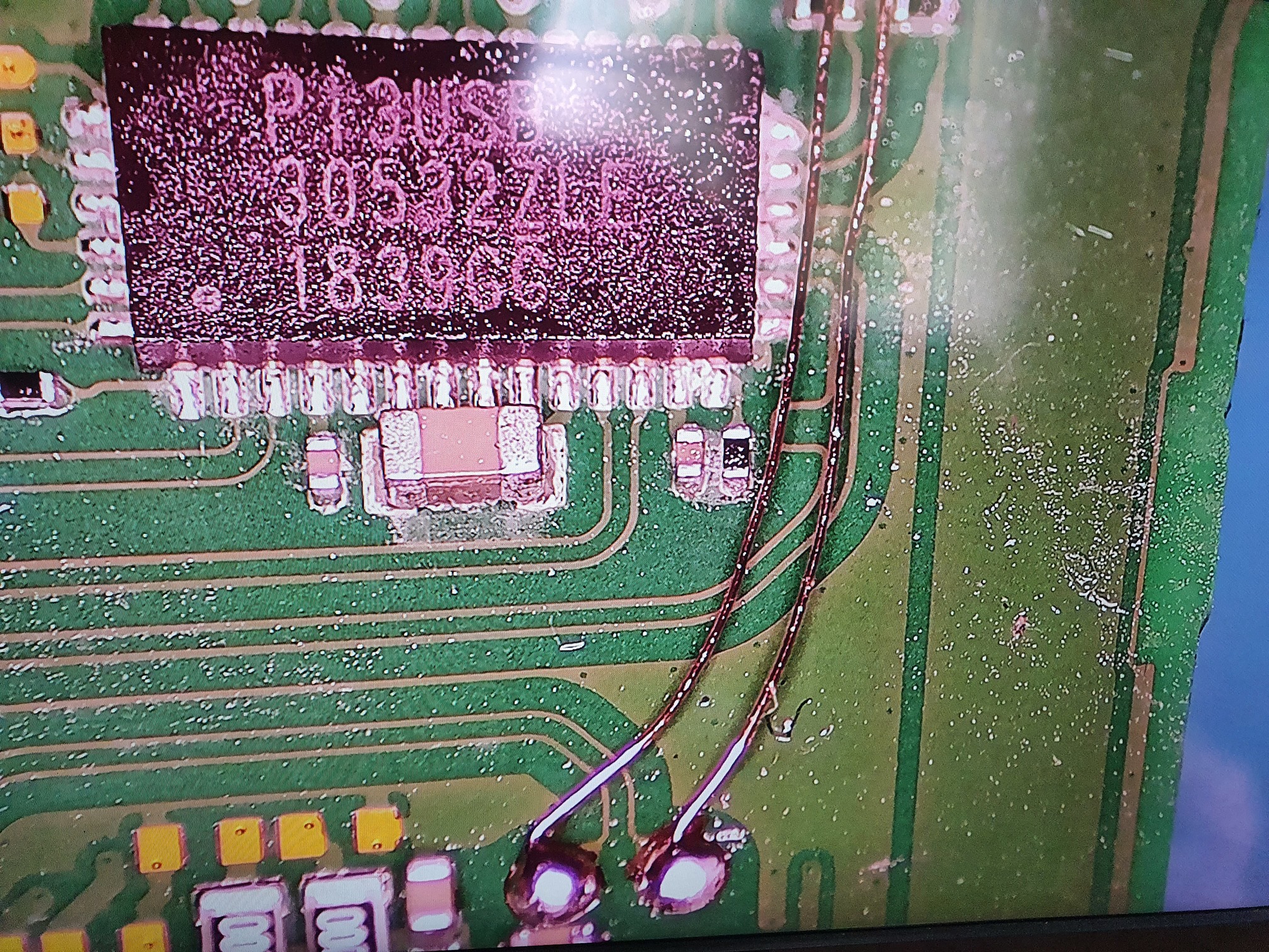
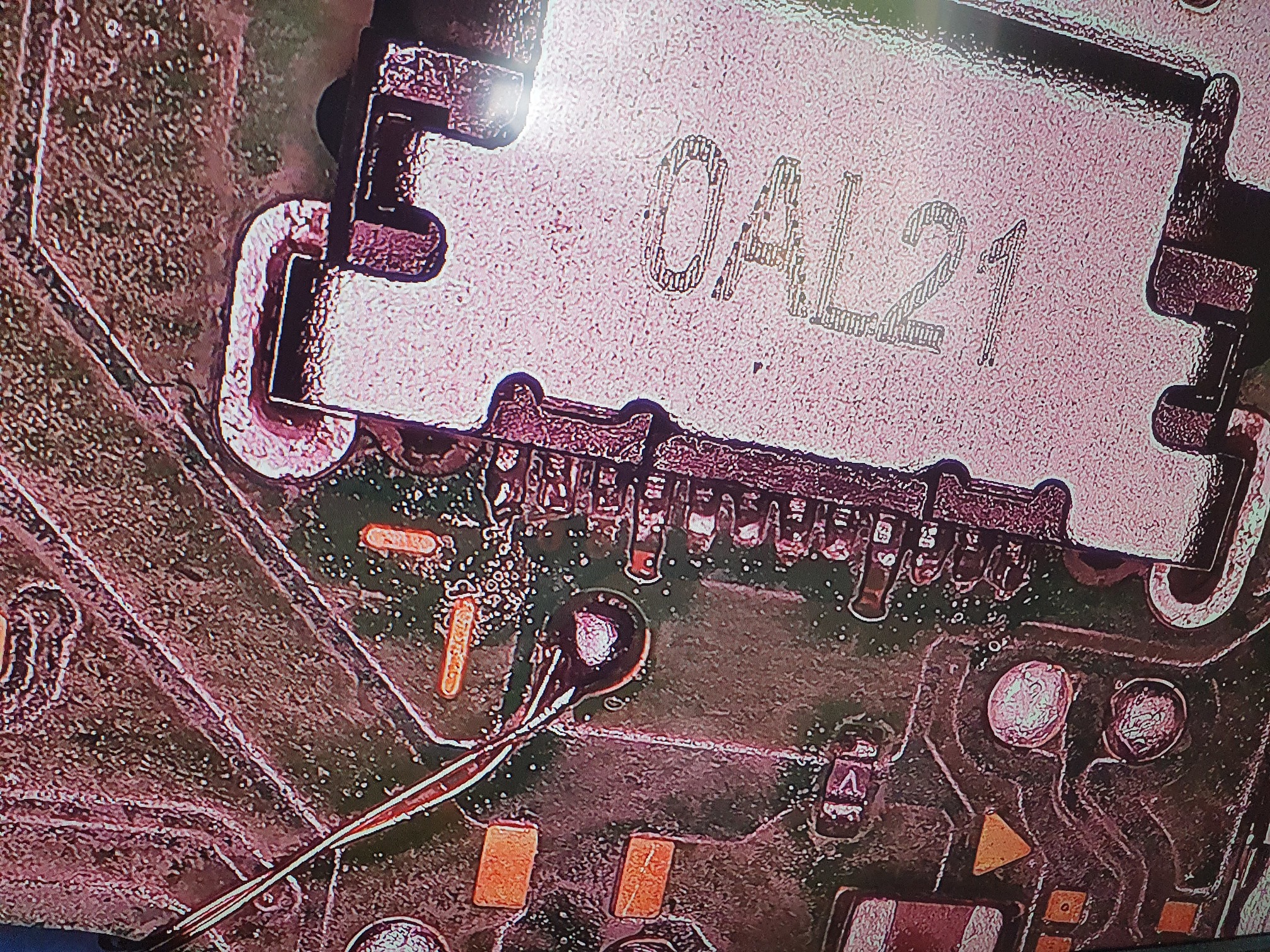
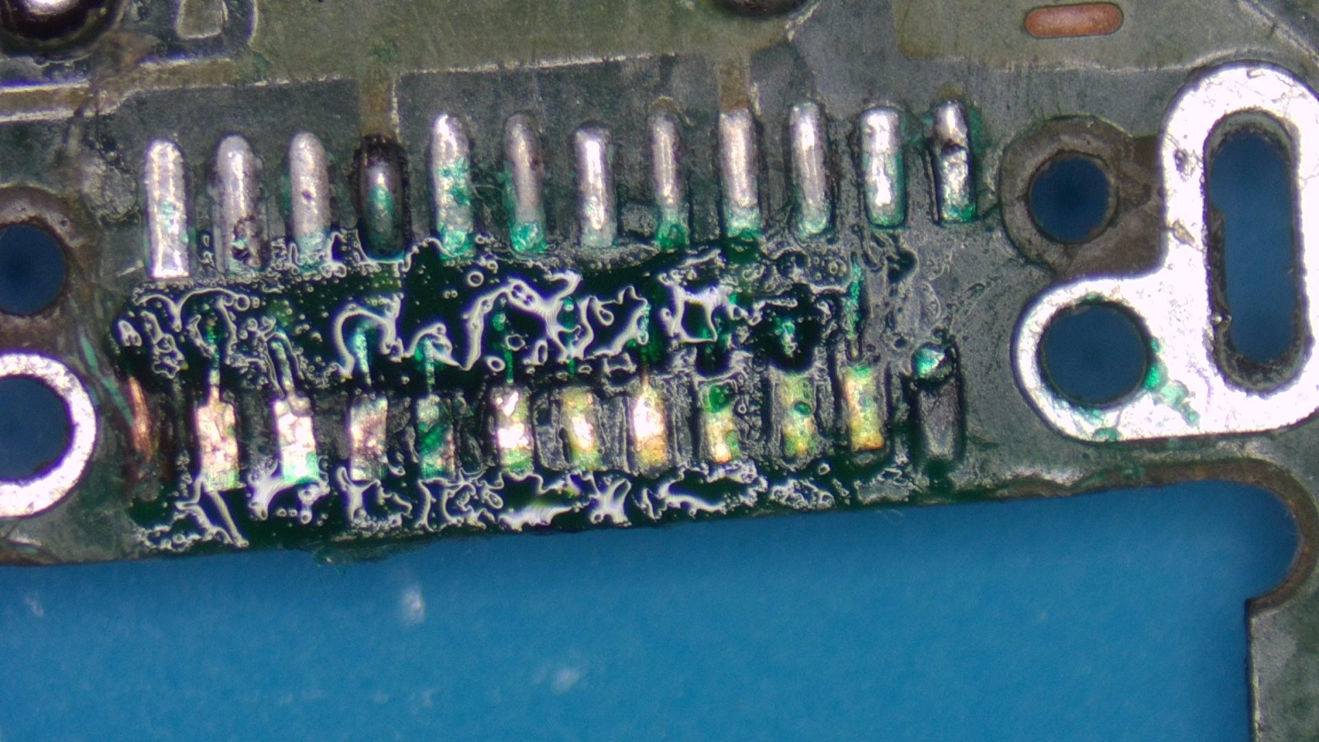
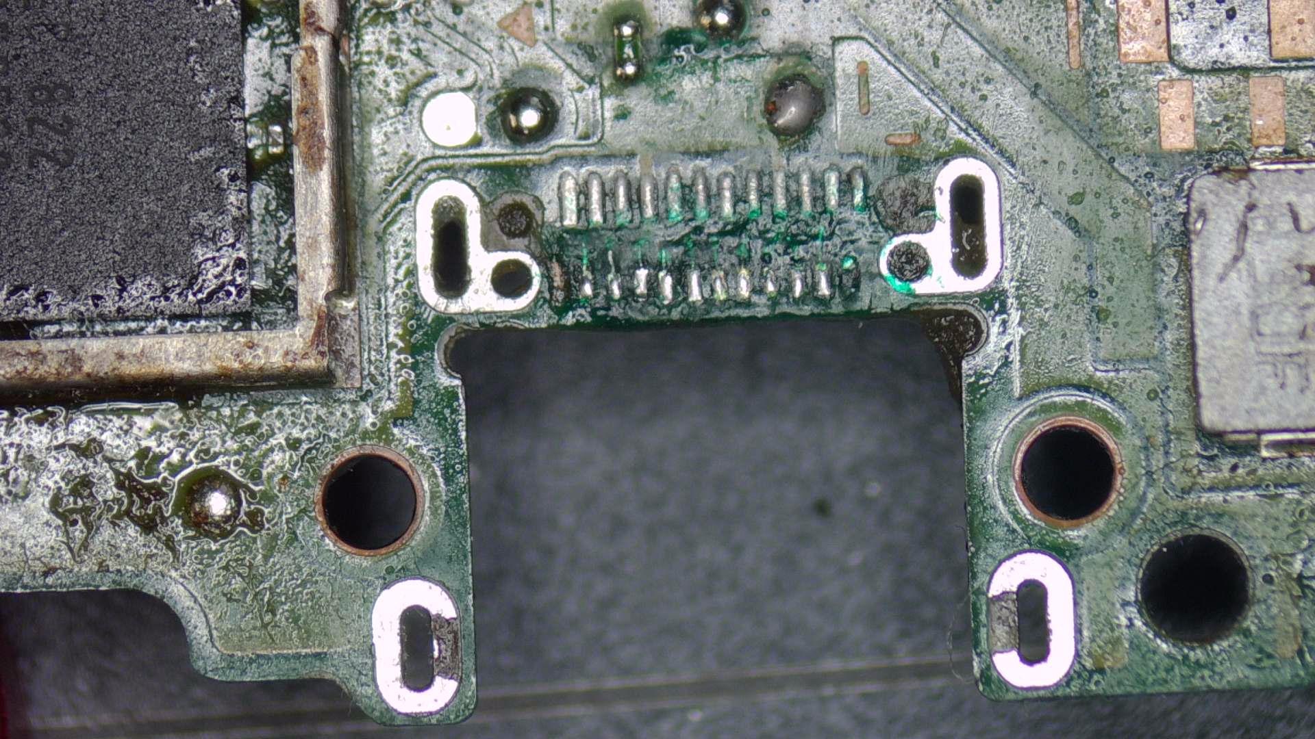
I made a row of mistakes during this repair, some of them were because I tried to find a workaround, since I had to wait for parts to arrive. Attached is now a series of photos with some comments.
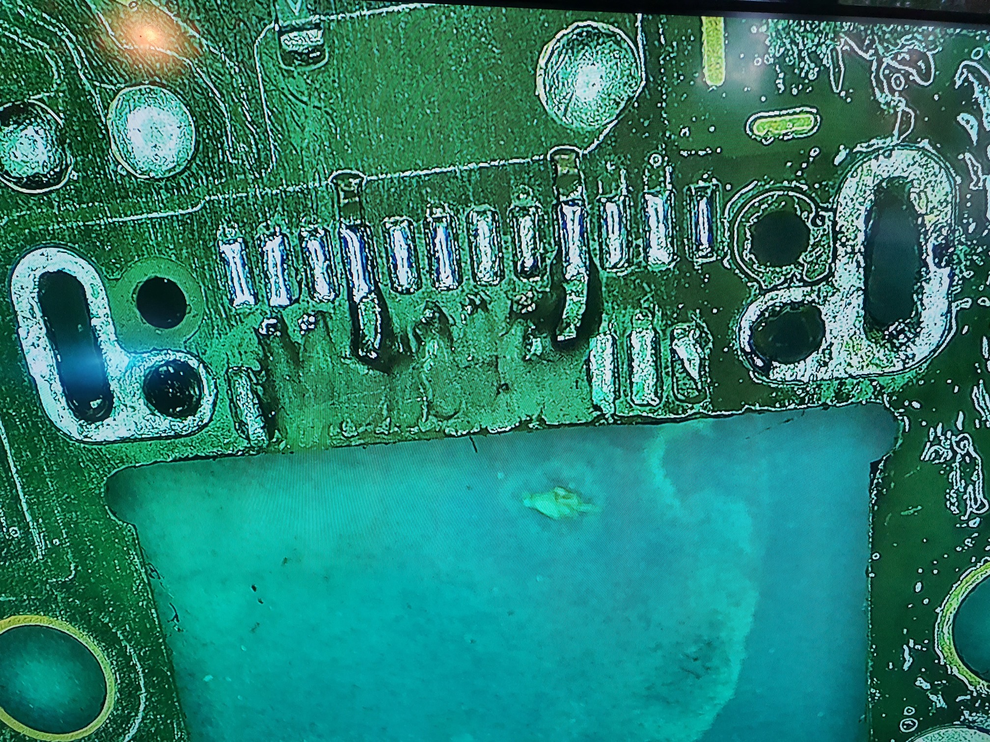
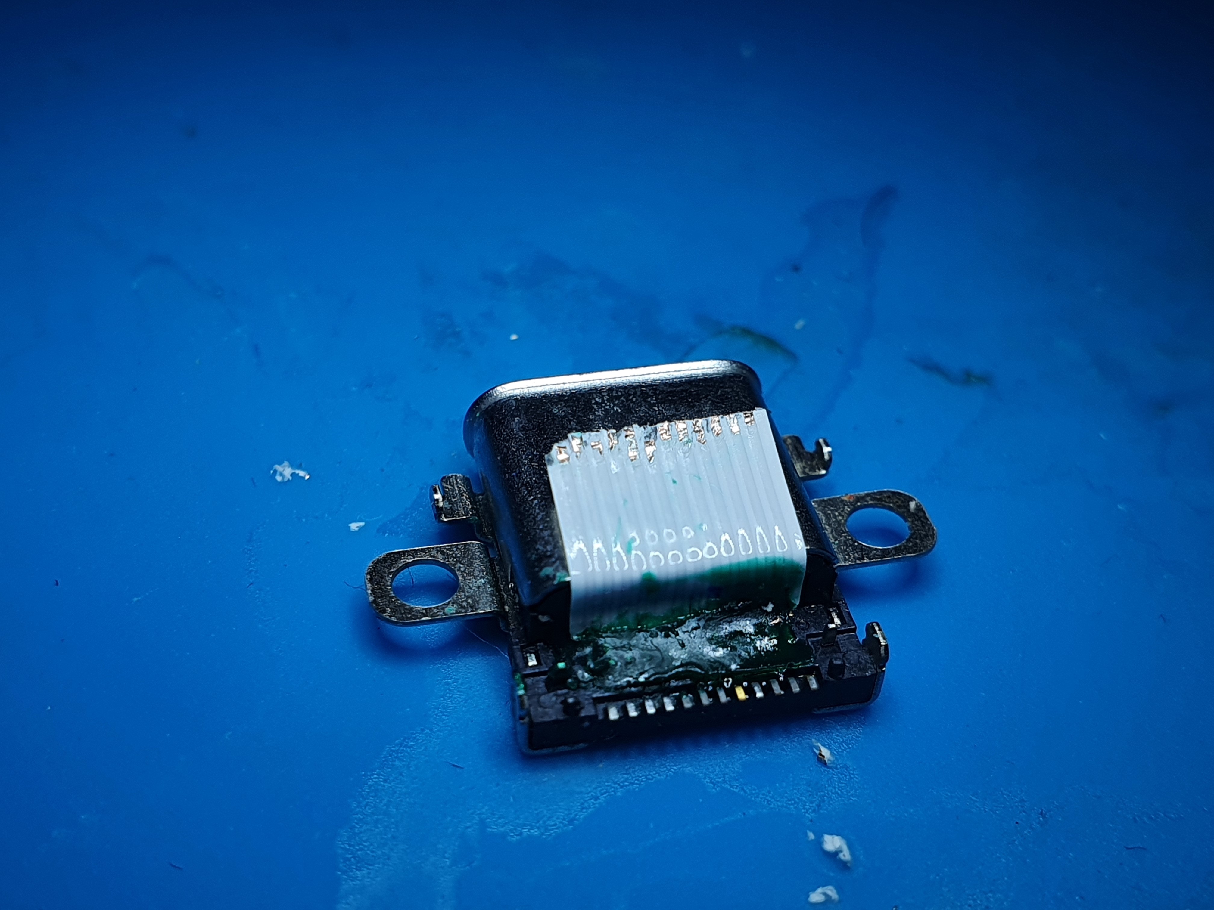
So this is mainly about the second (hidden) set of pins / pads of the USB-C port.
This is how bad it was:
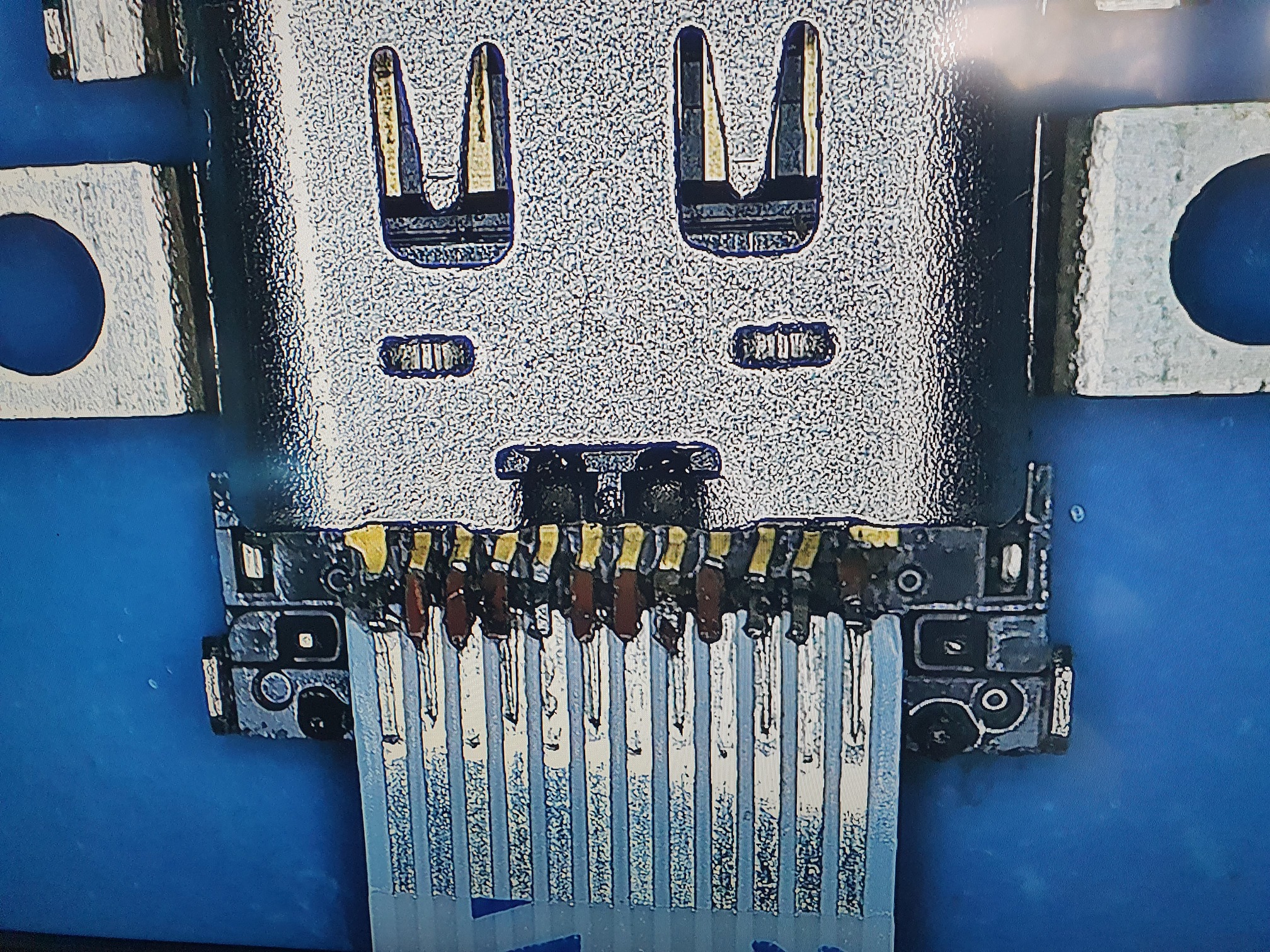
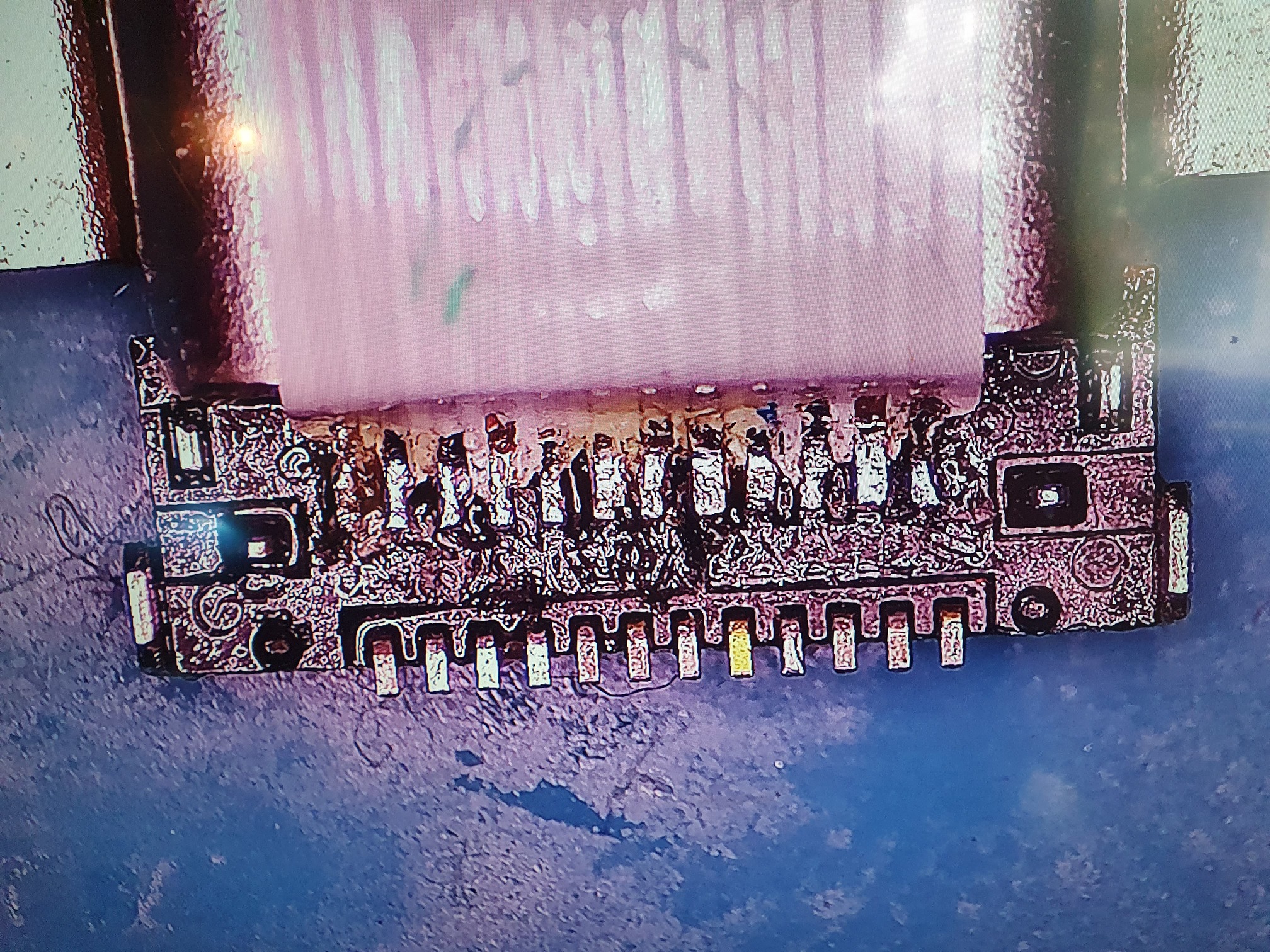
First I tried to slide the ribbon under the pads:
As this was not working too well (it wouldnt align to the board), I went with along with the method that was used here in this thread, … :
…covered it with some solder mask…
… and cut it and scraped off the ends:
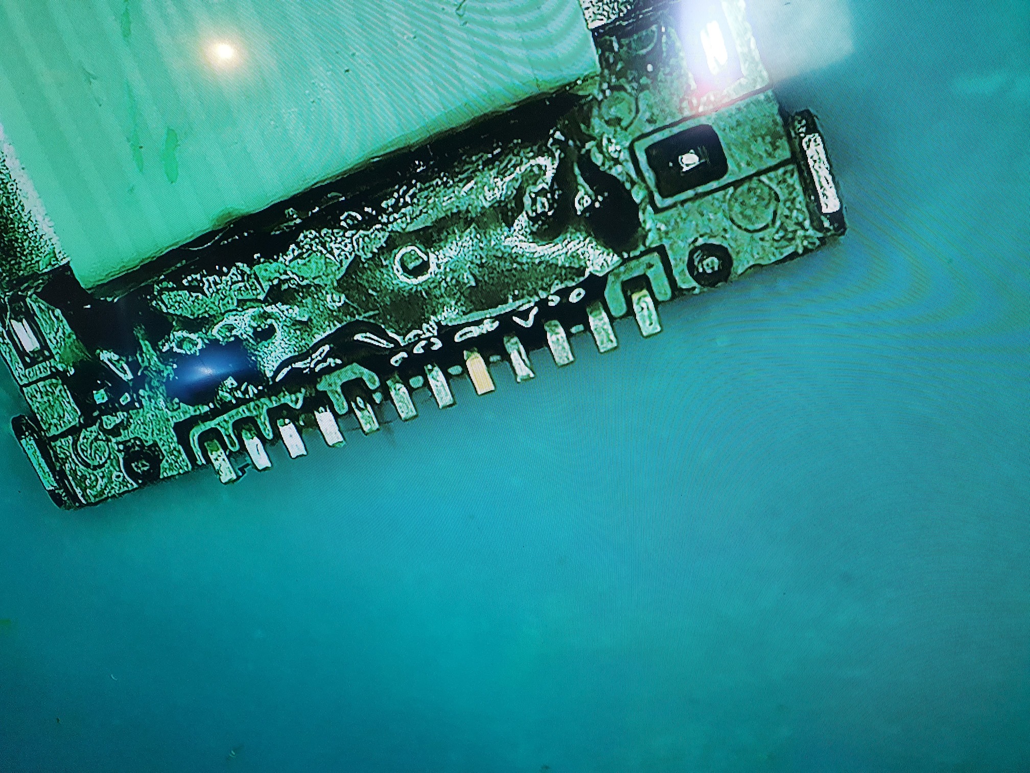
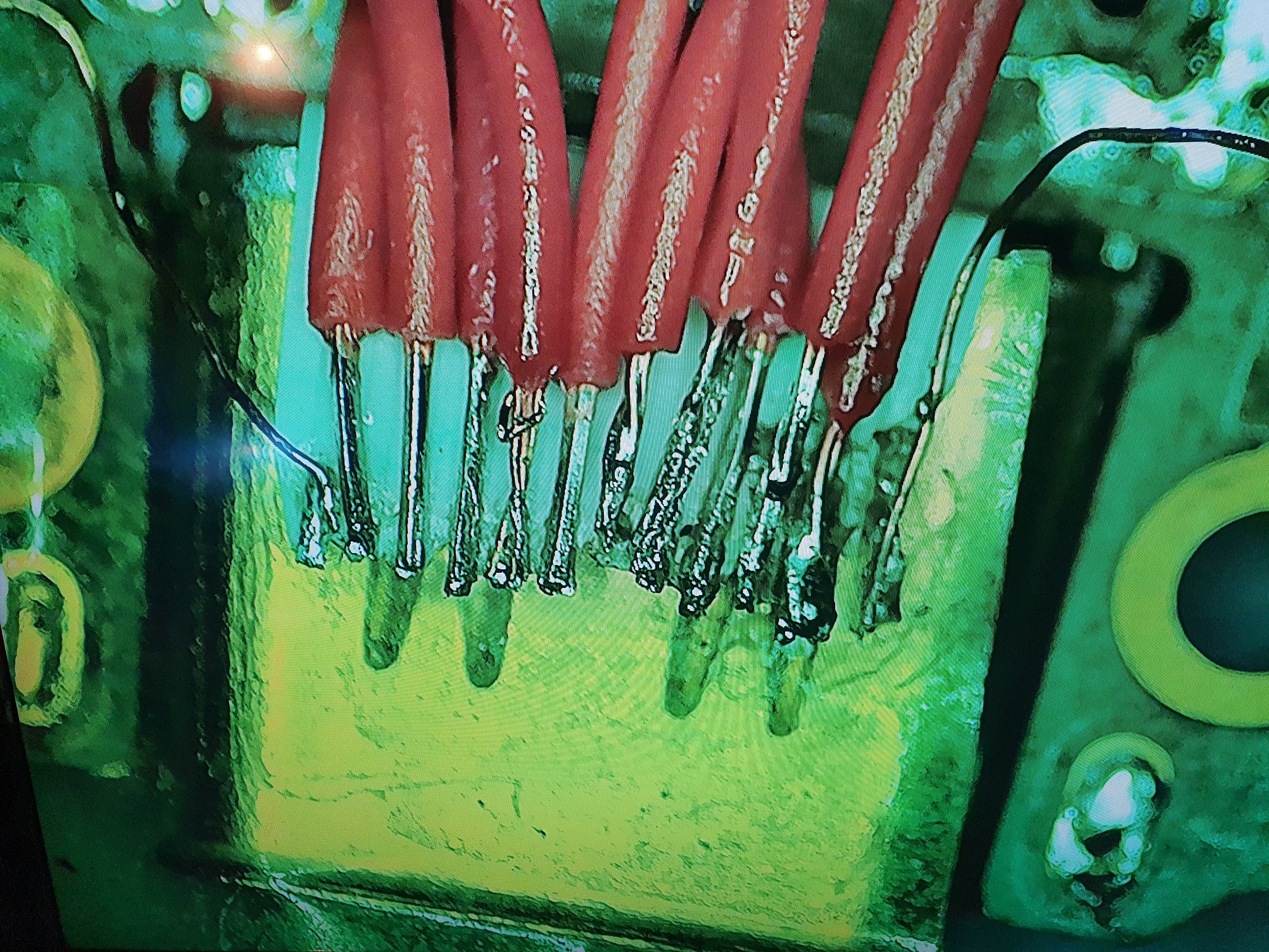
Now that I didn’t yet have jumper wires, I tried using the thinnest isolated wires I could find in my place and tried connecting them as shown by the author of this thread. I think they look a bit like sausages under the microscope =D :
This was a bad idea, as they were still to thick to put altogether back in the frame and have it aligned nicely. Also, it was nearly impossible to organize them in this tight spot and also to get them firmly connected to the tiny solder points on the board, especially the EMI filters before the P13USB. Some of them kept disconnecting, especially since the flex cable was not fixated and there were lots of small movements of the whole thing while working on it. So I gave it up and waited for my jumper wires.
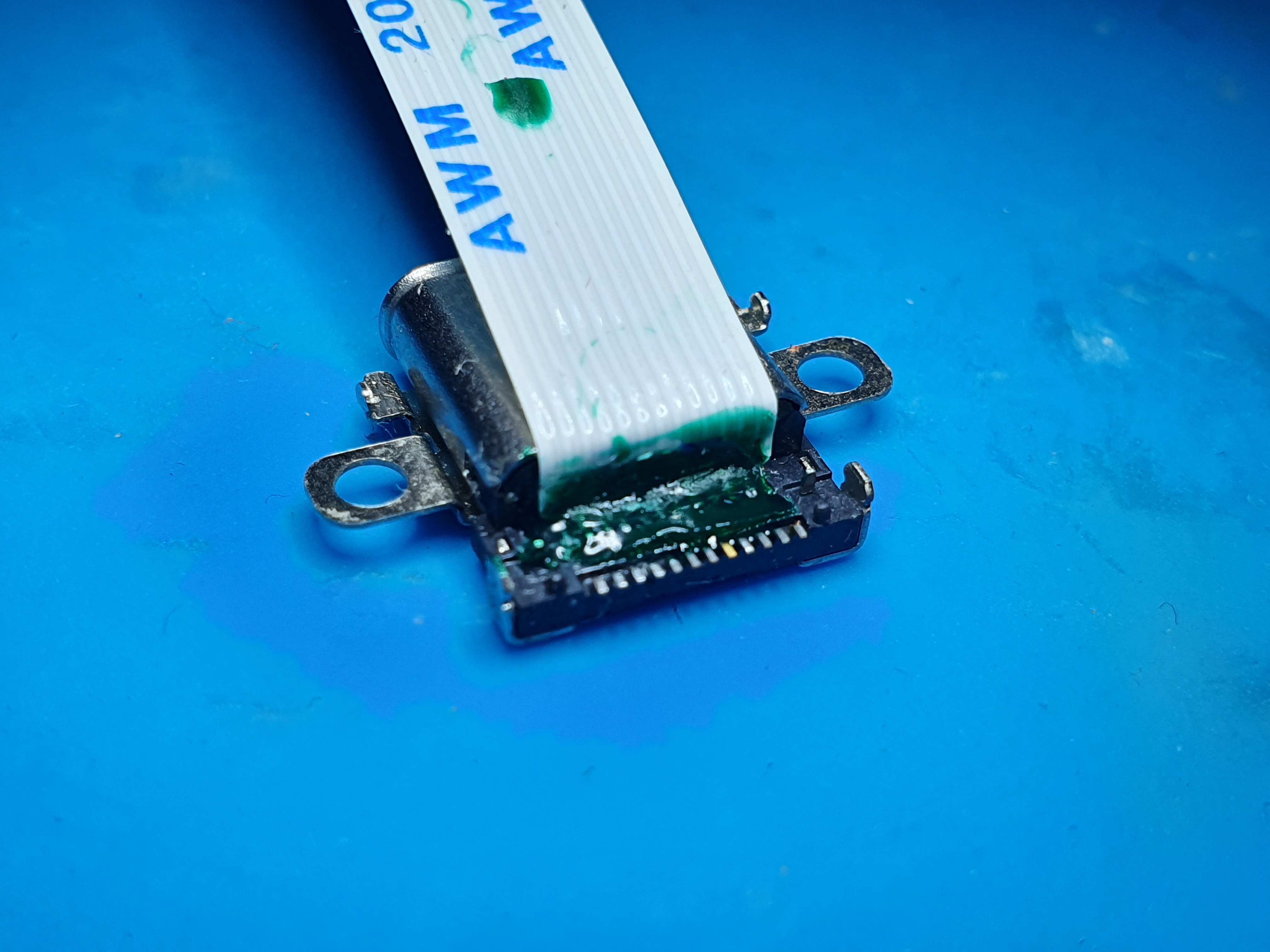
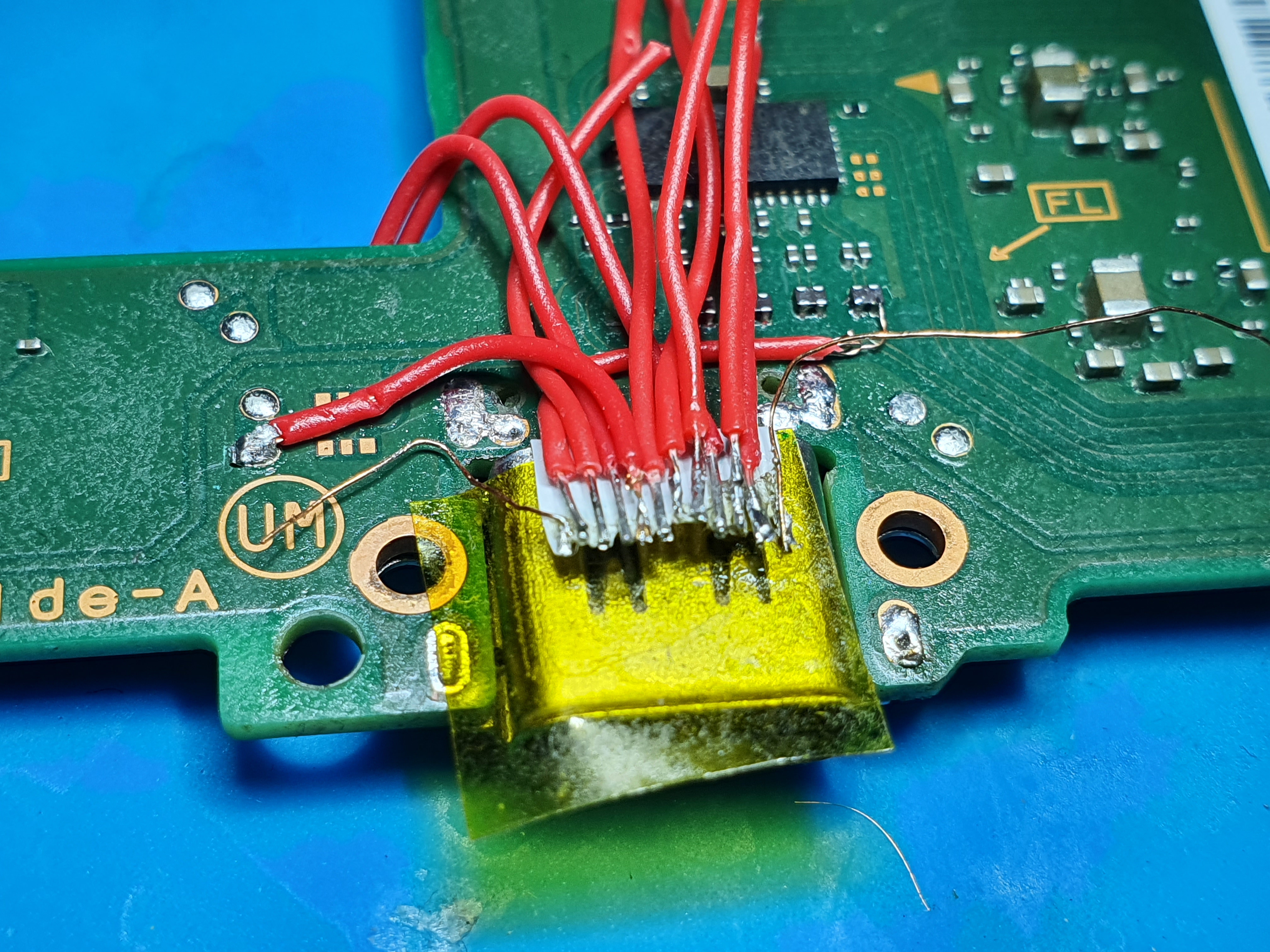
Muuuch better =) :
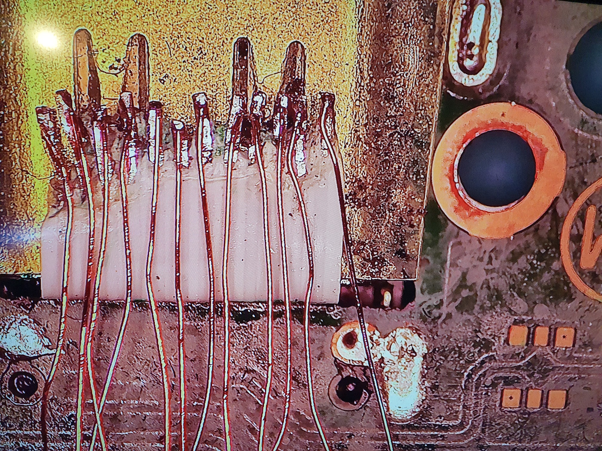
So here comes my next mistake. I took the wrong points. Luckily I realized that before connecting it to a charger ^^ :
OK so after correcting that and then testing the device, I found that it still wouldn’t dock. I checked some traces and points and found that one of the EMI filters had been damaged, probably a long time before already and probably as a result of bent pins of the previous USB port or a bad charger. As I didn’t have any replacement part for that, and I read a bit about these components, I decided just to bridge the traces accordingly. I am not sure about long term usage in this condition though. Also, lastly I applied solder mask on top of the flex and used some isolation tape between the flex and the port to prevent any shorts.
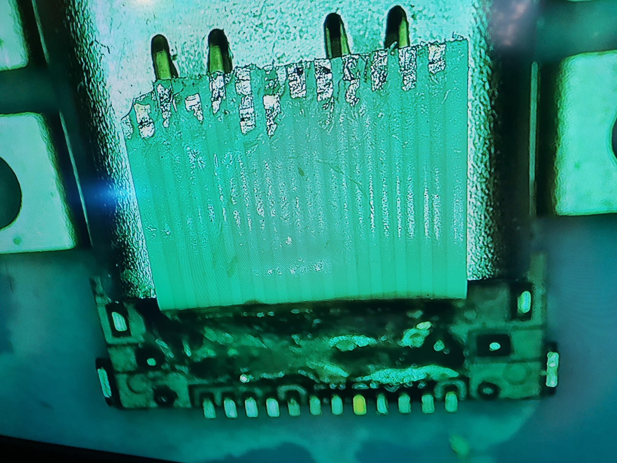
Another comment: after I built in the port, there was still some space between the first row of pins and the pads on the board. Probably my layer of solder mask on the second row of pins of the port, plus the flex cable, was too thick. However I was able to bend them all down to make contact and solder them to the pads. After lots of nudging and correcting, everything was firm.
Finally, the switch works, docks and fast charges. One issue remains; it only fast charges one way, if I turn around the charger, the current it draws is near zero, but it recognizes the charger. I’m not sure if this is maybe due to the missing EMI filter or maybe one of the connections between the port and the board has come loose again. I could check each point with my USB testing board, but as it docks and works and fast charges in the dock, I consider it as fixed for now =)
Thanks again for creating this thread, it helps us all to fix even the worst damaged USB ports =) Cheers!
damn, that looks complicated, congrats it worked out.
ill posted mine too, I have forgotten about it.
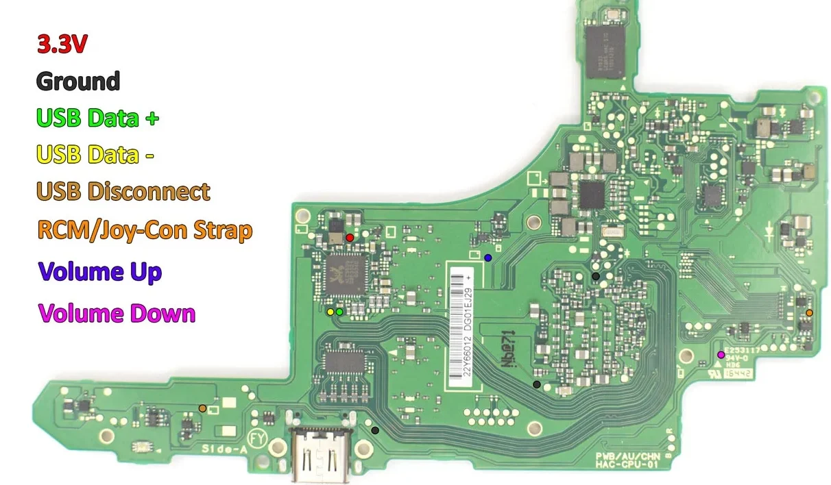
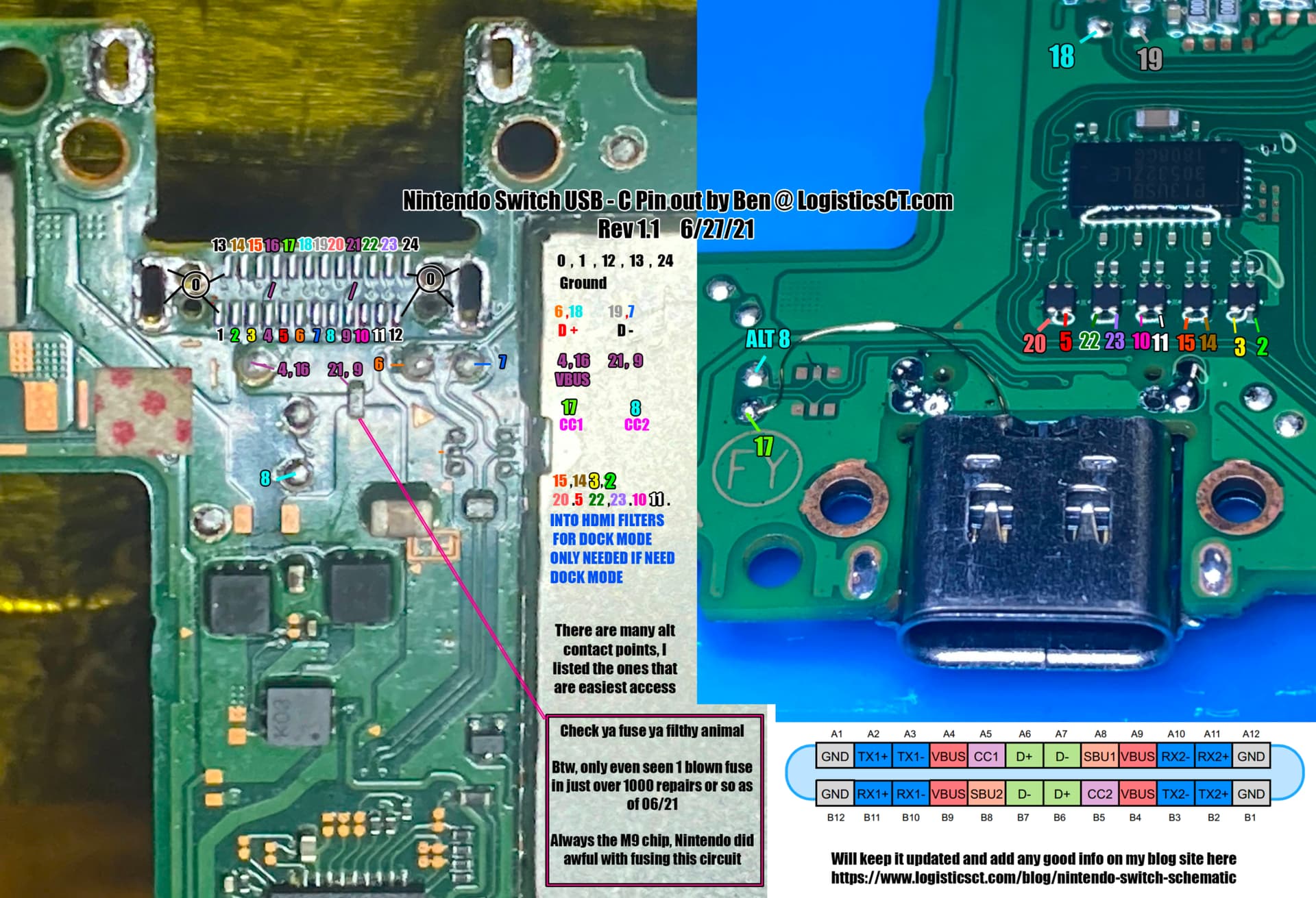
Thanks FXDX for all the connection points.
very nice alternative with the pad replacements, but I still don’t really understand how they would stick to the board. So I understand you cover the connection joint with solder mask, but the pad itself would need some sort of glue under it to make it totally firm? since if you put UV solder mask underneath, the UV light wouldn’t get there to harden it out… could you explain? Thanks!
I have used JB-Welds steal / metal epoxy before, as it has a high enough heat tolerance for soldering. But you don’t really need to, those pads are not structural, that’s what the legs are for. As long as it is able to make connection you are good. It just needs to stay in place long enough for it to be flowed in to place.
Another thing I realised is, that after putting it all together like in @FXDX 's layouts, and testing the points on my USB-C breakout board, D+ (A6) showed continuity to D- (B7), as well as D+ (B6) had continuity to D- (A7). Testing the breakout boards with other known good Nintendo Switches, continuity always is present between D+ on both sides, and D- on both sides. After swapping the solder points 2 and 3 (reference: FXDX’s picture of side B), continuity seems to be correct (?). So I’m wondering if there would be a difference in board revisions, mine is HAD-CPU-001, or I am not sure if I understand the wiring…
There is no difference between the motherboards. There may be a mistake in the picture side B, between the D + and D- points on the motherboard and D + and D- on the test board. It is possible to reverse the points between them.
I had a console with all the bottom usb c pads ripped off, and I used the second method to fix it. Now the console works but does not dock and only charges one direction. I thought I messed up my soldering, but I have now found that CC1 has a direct short to ground. I traced the cc1 pin back to the m92t36 chip. Should I try replacing the m92t36 to see if it will start to charge?
In my opinion, it has something to do with the port itself. I had exactly the same case some days ago, and i just create a short underneath the port which causes exactly the same issue as you. I used stripping pads in my case, and just placed a bit too much solder on the pads or not enough flux, or maybe both  But i don’t believe in coincidence, or at least not in this case, but still i may be wrong
The reason I blamed m92t36 chip is because the short was on the top side pads, not the hidden ones. I dont have a new chip but I transferred the chip to a new console and the new console only charges in 1 direction now. I ordered a new chip now to replace it, we will see if the issue is solved.
Hi. My board is had-cpu-01 and I’m trying to figure out if the alternative test points (Side B) D+/D- are the same. I saw this picture which they are reversed.
I think there might also be a mistake regarding TX1-/TX1+ and RX1-/RX1+ which seem to be inverted in your diagram.
That one seems right:
Quick question to everyone: I have this switch with ALL THE PADS gone (whoever worked on this was a little brutal). I got it to charge on both sides, but I’ll be happy if it docks at least on one. I’m currently running wires dead-bug style from Side A.
It’s not working though. Why? Do you need both sides for HDMI ?
(By which I mean: do you need both RX1 and RX2 for instance, or is one enough? I have a feeling you need both)