I decided to open this thread in the idea that it will be useful to the community of this forum.
I am not an electronics specialist, but i have some years of experience in microsoldering and especially in reballing. I have seen that there, are enough users who have faced in the process of repairing Switch with pads removed from motherboard in the process of replacement the USB-c port. This happens, when the person performing this operation uses inadequate tools or incorrect settings of the hot air station, namely temperature, the air flow or the flux. I am trying here to present two methods of reconstructing the missing pads from the motherboard to the usb-c port. None of the methods belong to me, i also found them on the internet and used them successfully in the in the repair process with destroyed usb-c pads.
The first method.
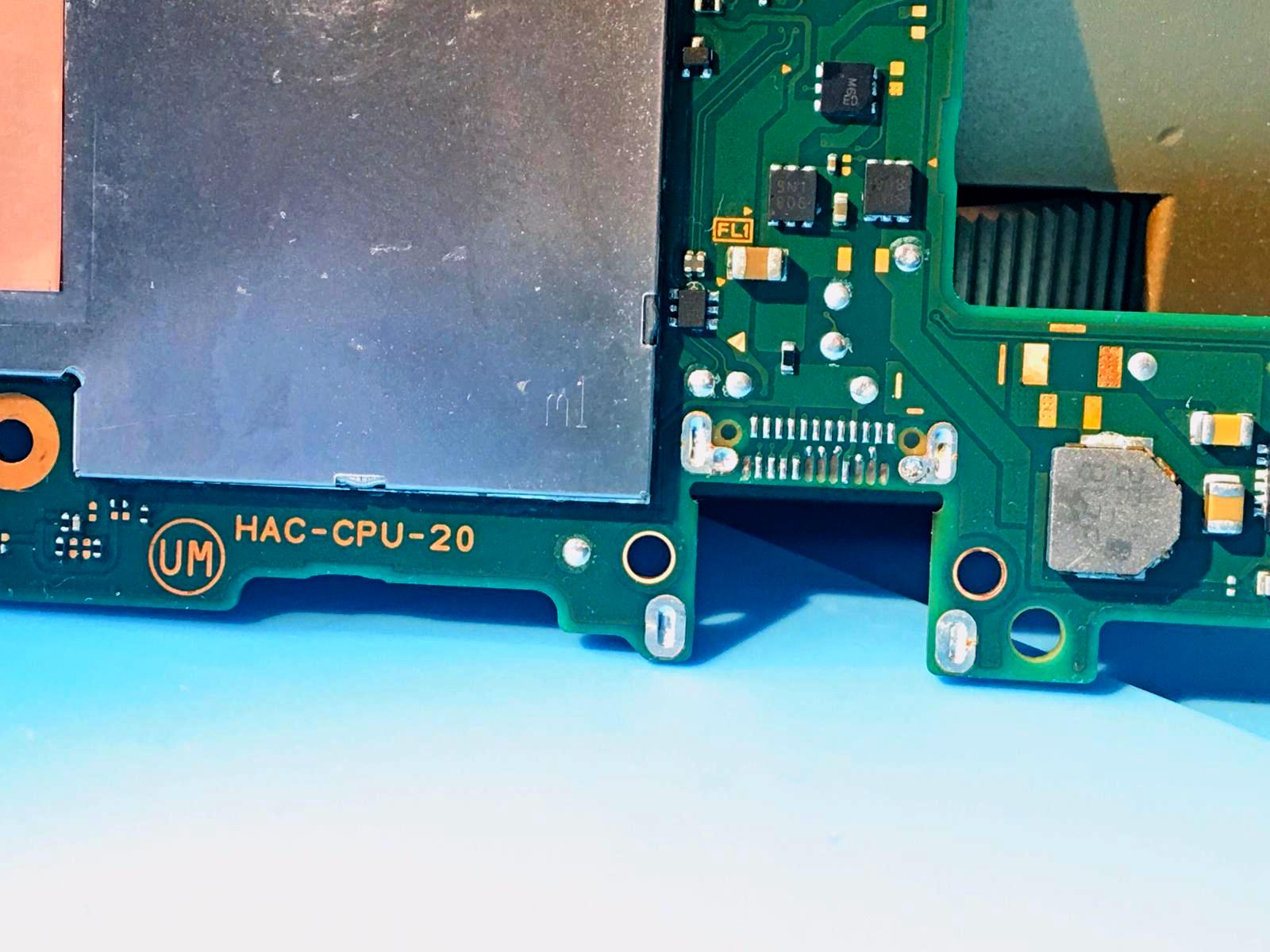
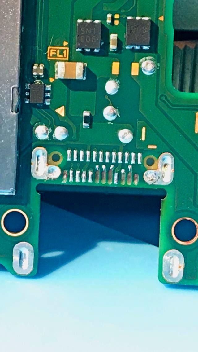
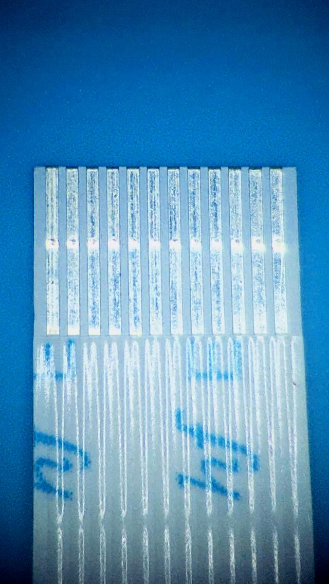
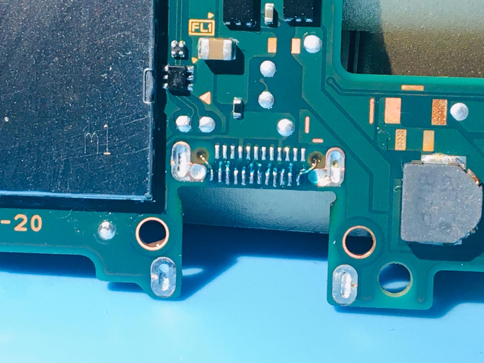
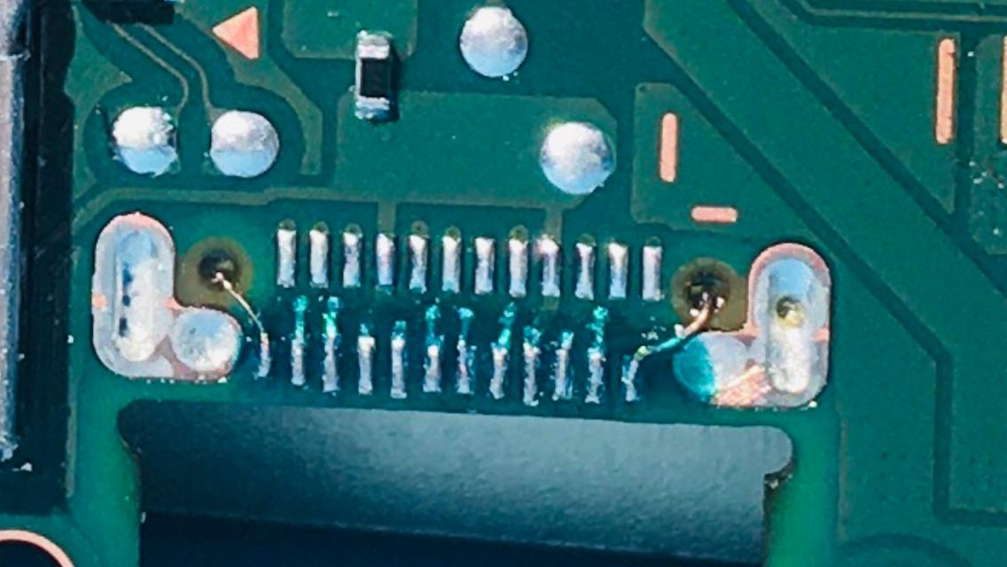
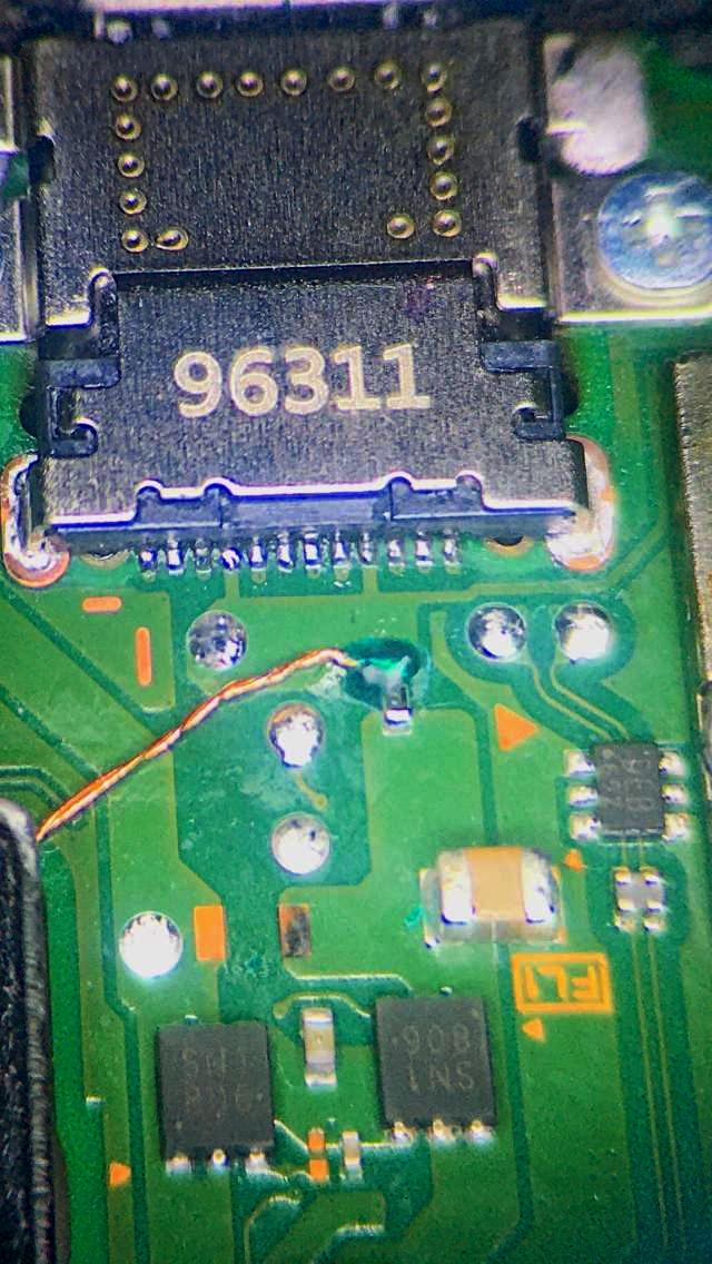
I used a connector ribbon cable and under the microscope i cut the small pieces of copper after i previously peeled them with a cuter, about the size of the original pad left on the motherboard. I scraped on the logic board of the switch with a surgical knife in the place where the pad was lifted until i removed the solder mask that covers the circuit and i managed to make the circuit visible. I put a little flux and with the soldering iron i put the tin on the circuit. Then carefully i put a piece of cut copper in the place where the original pad was and carefully fixed it with a little UV solder mask, which i dried quickly with a UV lamp. Then with the soldering iron i made a bridge with tin between the circuit and the new pad implanted on the board. That is how i proceeded to all the lifted pads.
Method two is a bit more complicated.
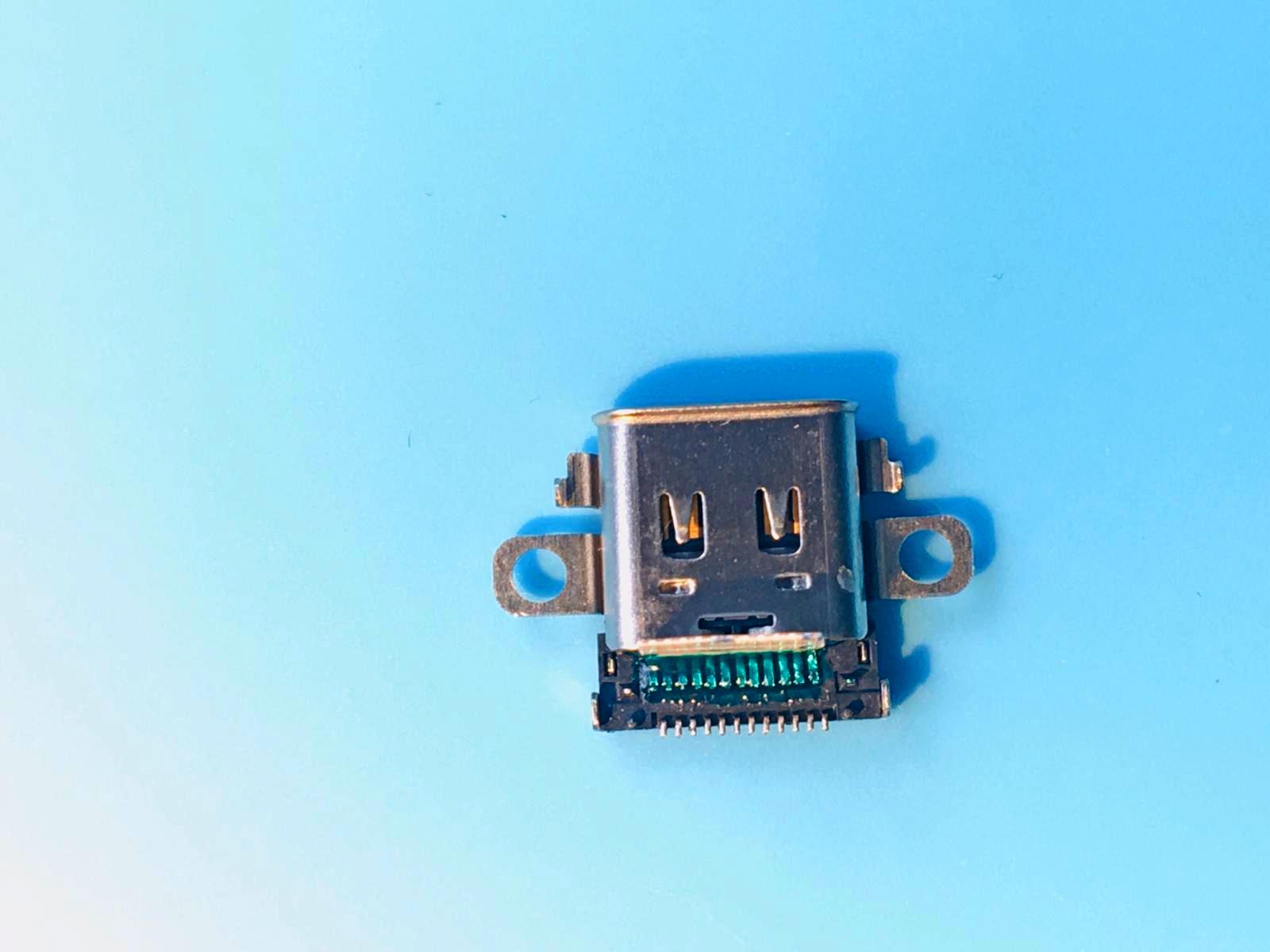
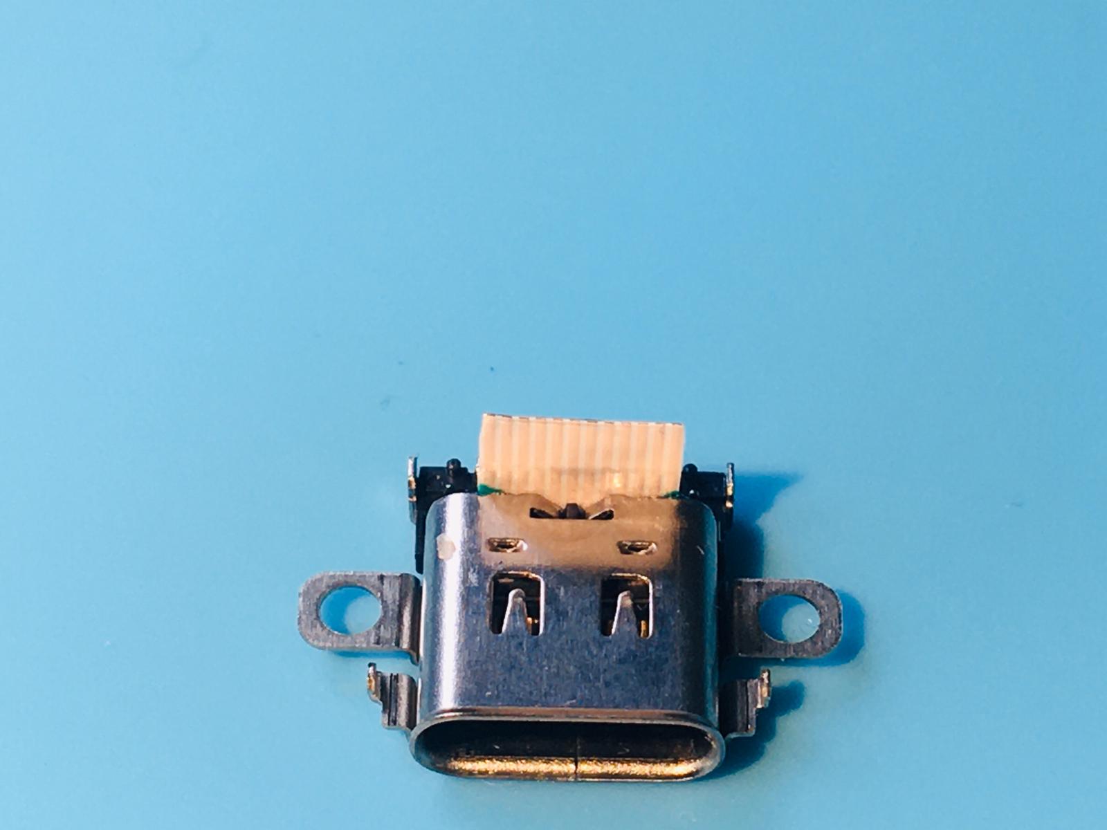
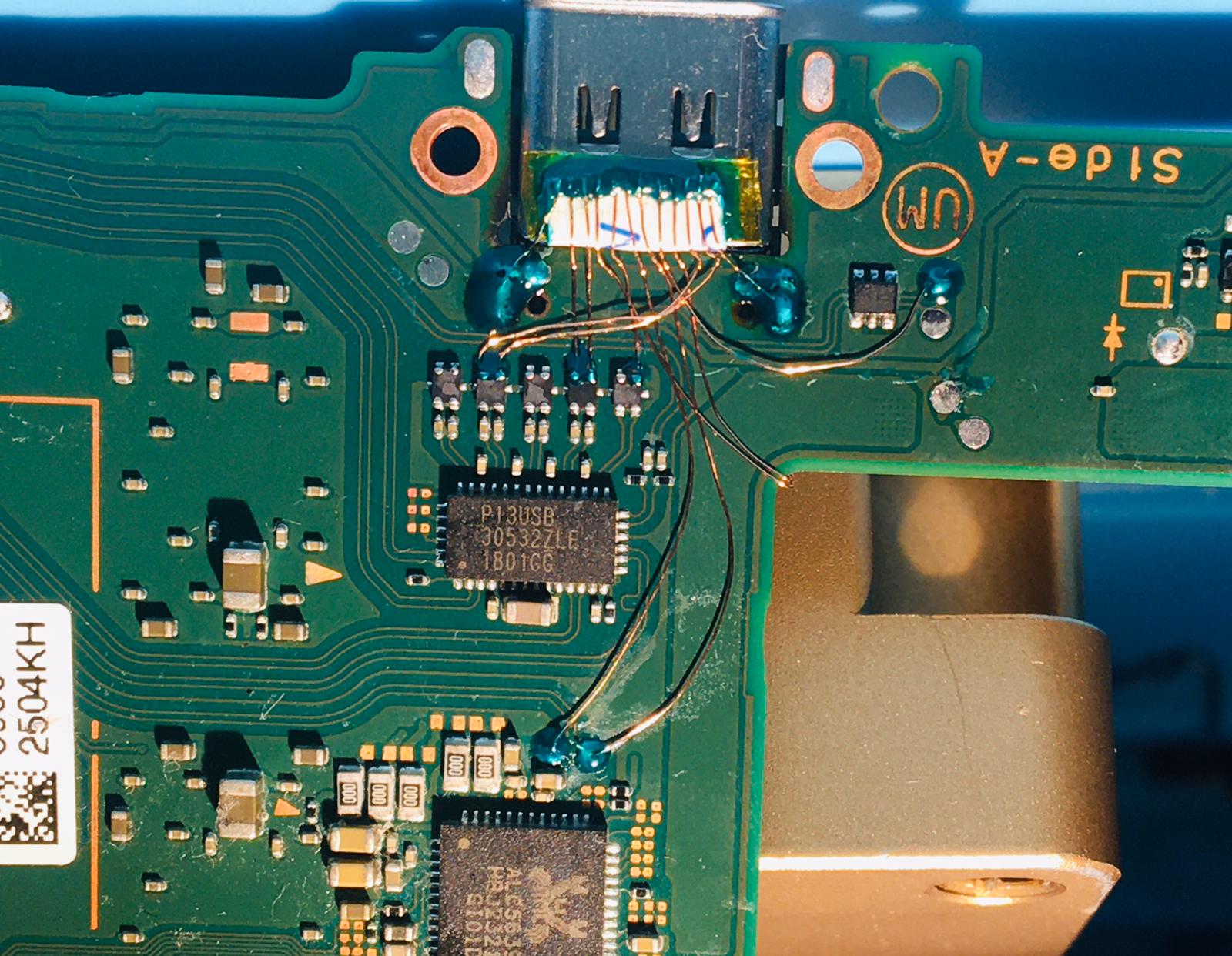
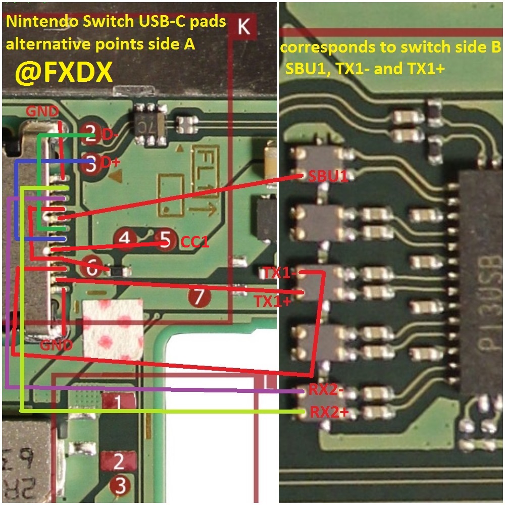
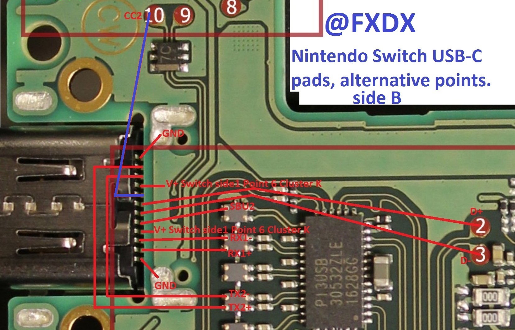
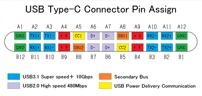
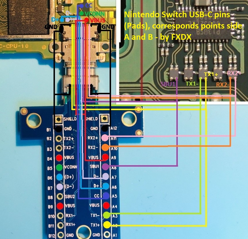
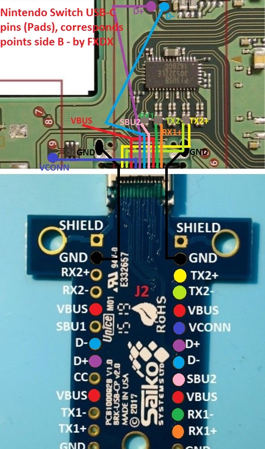
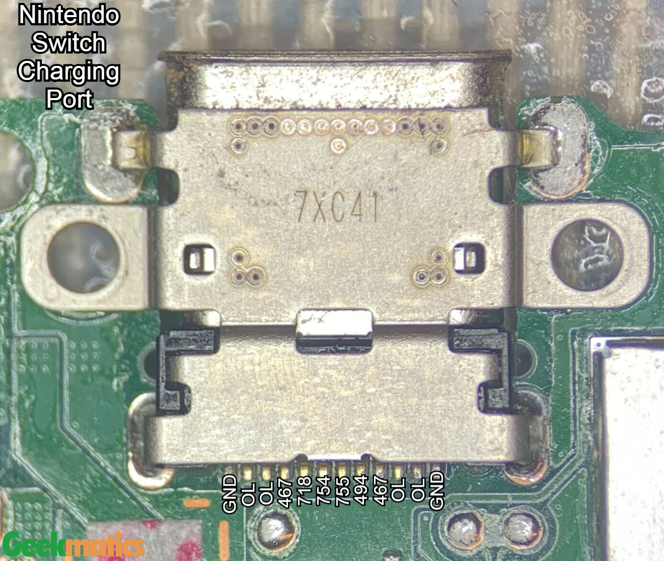
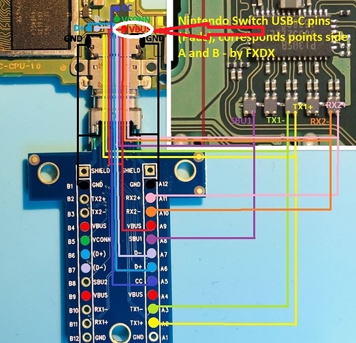
I cut 15mm from the connector ribbon cable and under the microscope, with the soldering iron i solder the circuits directly to the pins on the usb-c port. I mounted the usb-c port on the motherboard and the other end of connector ribbon cable i stuck it on the other side of the usb-c port. I scraped on the ribbon cable and i managed to make the circuit visible. Then i pulled wires from the ribbon contacts to the alternate points on the motherboard as in the diagram below and i isolated with UV solder mask.
Both methods require patience and good microsoldering tools. A microscope or a good magnifying glass will require for a successful operation.
I apologize for my bad English and i hope it will be useful for what i have set out here.
Interesting post! In response to the second method, could one lift the second row of pins on the port to make easier to solder the ribbon cable without the need to flex the cable?
There’s a YouTube video that shows repairing of the USB-C port. I can’t post links but the title of the video is: Nintendo Switch - Charging Port Missing Pad Repair
The type I am getting sent are not “exactly the same” as the original port as the original you can access the hidden pins from underneath slightly. The ones I have been sent you can not.
Did you modify the port at all when using the ribbon cable?
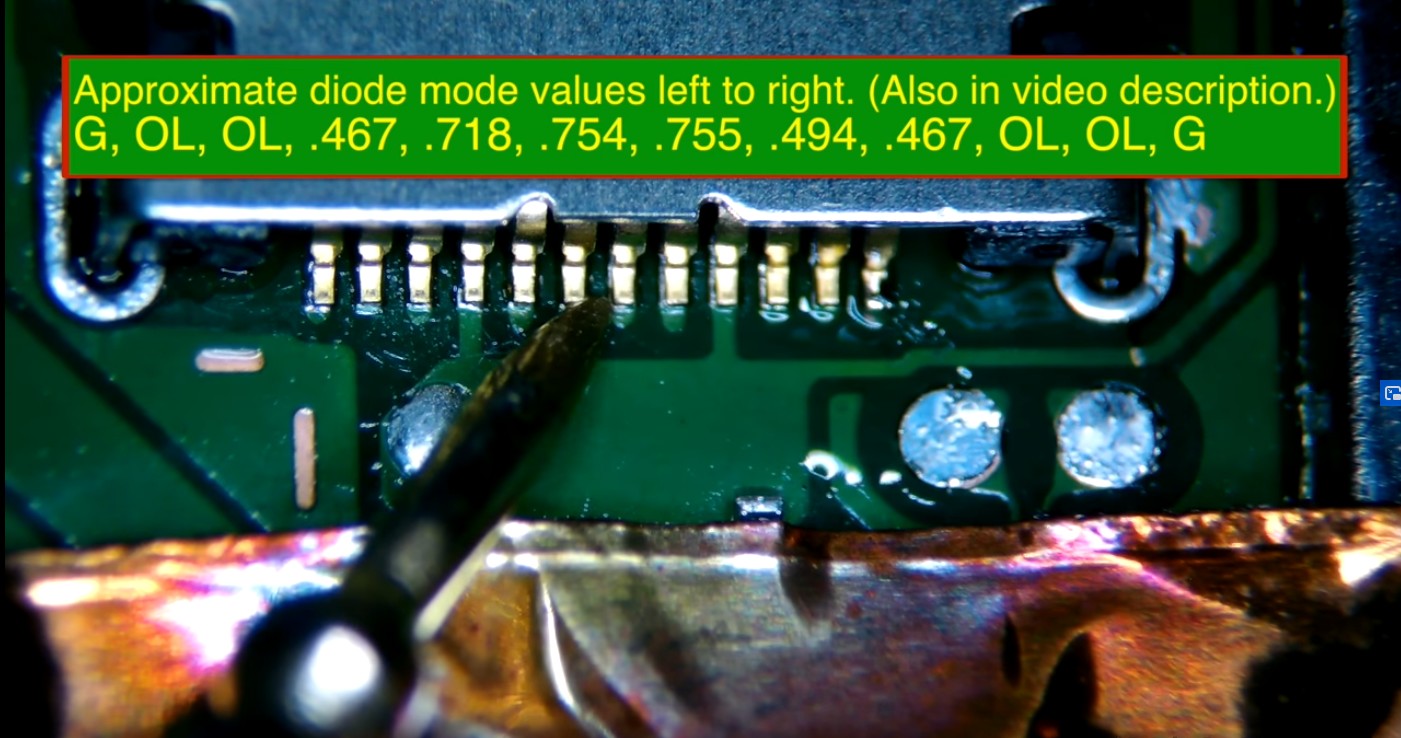
I have managed to solder a ribbon cable onto the hidden pins row, I’ve checked for continuity/shorts/bridges seems ok, I will attempt to jump wires to the alternative points when my solder mask gets delivered.
fyi, in your original pics you can dig out the two outer ground pads which you ran the two enameled wires via the holes. It’s just ground plane below so it’s safe and neater.
You look amazing.
I tried in the same situation, but I forgot that only half of the usual solder was attached, and because I connected the adapter strongly, the other half of the pads were also removed.
Needs more careful treatment