Hello everyone, I got a cheap switch tablet off of ebay and I tried fixing it.
Initially I found shorts on 5 caps around the M92T36, and when plugging in the charger with a USB C tester, it would not turn on, making me think there is either a problem with the USB C or some short on the power rails.
Fast forward, I replaced the USBC connector and the M92 IC and the shorts are gone on the caps around it, but the USB tester is still not turning on. After this by looking around I found 3 caps shorted to the left of the MAX chip and 4 caps shorted under the ram/soc area. So at this point I am just thinking it’s fully dead, anyone got any idea?
I tried measuring in diode mode to see if the values on the caps were matching a picture I found on the forums, however, from past diode mode used, I noticed my multimeters never matched online values even on working devices.
Please let me know if I am missing something or anyone has any idea.
Separately, I have tried attaching pictures of the shorted caps but I am getting a “You cannot embed media items in a post” error.
they’re not short, they’re low impedance cap. Need to check resistance to ground as well as listen for beeps.
Nothing on meter means your work on M92 is probably poor (or the chip you replaced with is faulty / fake) and needs a touch up, your USB port work was poor and needs a touch up, or the fuse above the USB port has blown and needs replacement.
Hey there, thanks for the reply.
The fuse was fine, I had already checked for that.
I have checked the voltage on the battery and it was 2.4v. I decided to charge the battery outside of the switch with a universal battery charger and after doing that and putting everything back together the switch turned on but only the backlight was on, nothing on the screen, couldn’t head any sounds, couldn’t hear the “click sound” when you use the touch on the lockscreen.
Went into RCM mode and it was detecte into RCM, and the payload got injected without issues. But still no screen.
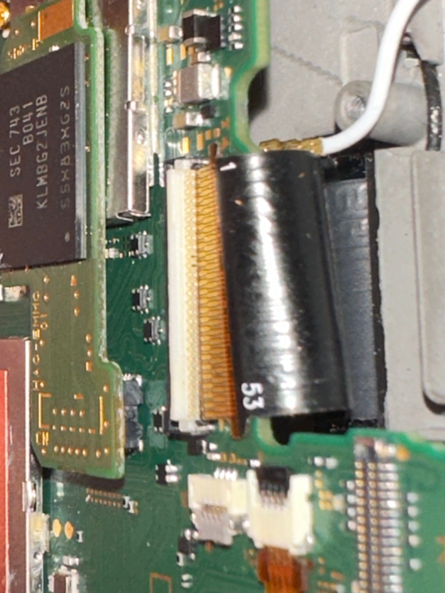
So I decided to look at the pins of the usb c and ftp lcd connector. Turns out the USB C can be lifted at an angle for 1mm easily, and the fpc seems to have 2 pins missing but I am not sure if it’s supposed to be like that or the pins are actually missing. I got a 2nd screen so will give that a try tomorrow.
Pretty angered about the USBC as I got it replaced by “a professional”. And it looks like some of the pads are ripped too. So I’ll just have to do it myself and just redo the traces. Although I find it interesting the traces that are there are enough to connect to PC and inject the payload, but not for the USB C tester to turn on.
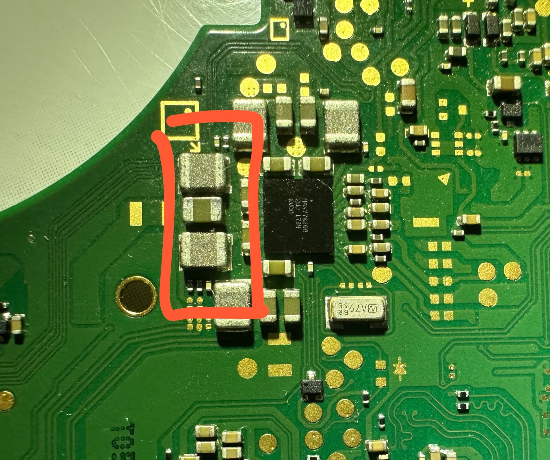
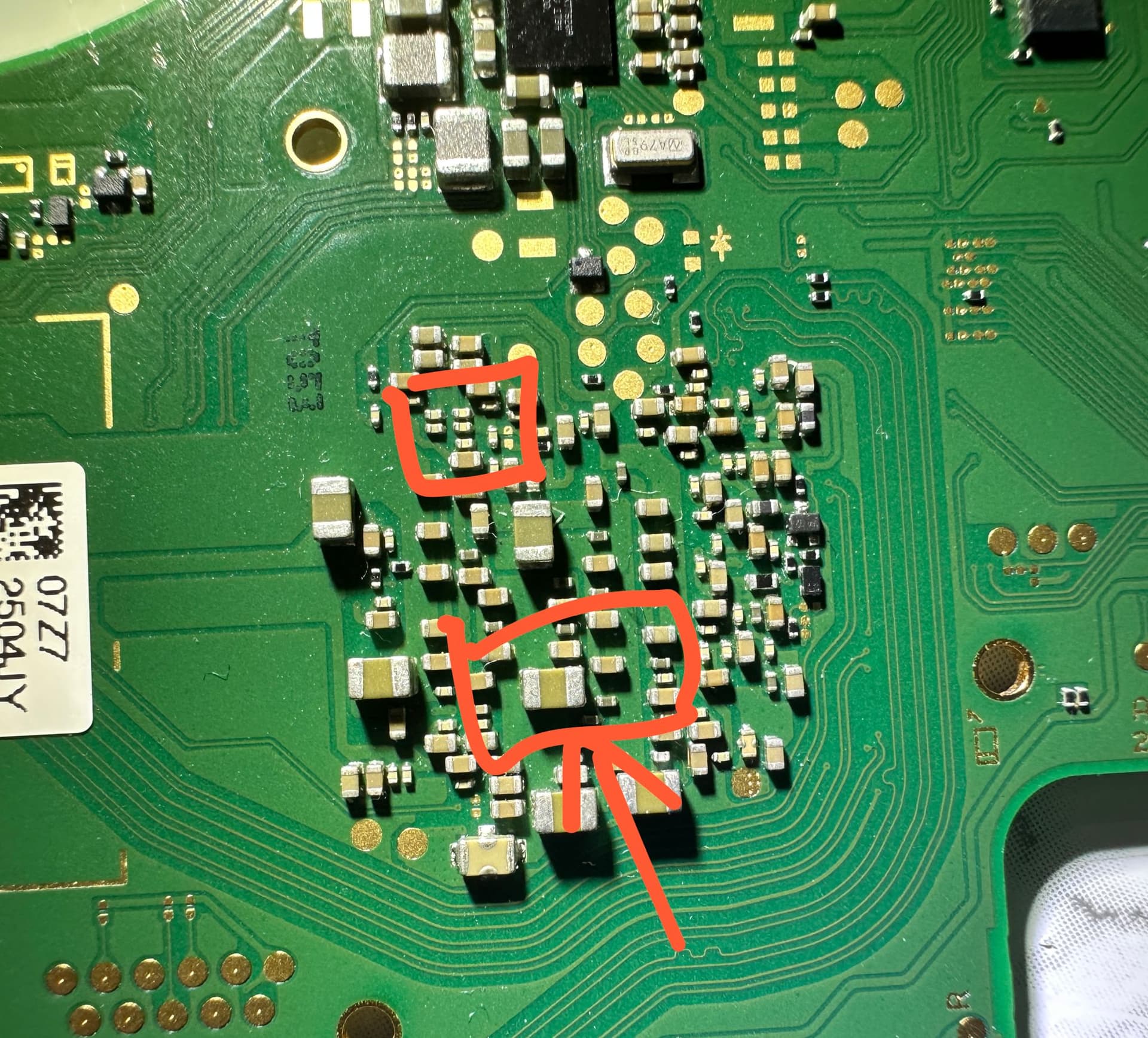
Now that I can actually post pictures, these are the 2 areas with the capacitors that show continuity with ground, although you mention them being low-impedence.
I don’t understand why everyone answers these forum questions as if they are talking to imbecils.
It is obvious that a 2nd display won’t work if the display fpc connector has missing pins. The reason for a 2nd display being used for testing is because I do not know (as the switch was bought used from ebay), what they did with it and what works and doesn’t. Separately, some pins in the FPC connector are not used, so the 2 “that I think are missing” (because I do not know if it’s supposed to look like that or not), could end up being part of the non used pins.
I do have a 2nd display, and I don’t have a replacement connector, so it’s an easy test, before ordering one, and having to desolver/solder a new one.
Top image is definitely low impedance, should be between 28-48ohm to ground depending on board revision
bottom image are most likely low impedance as well since those caps tie directly to APU.
With both areas turn off continuity and measure the actual resistance, if its less then 1 ohm you have a problem, if its in the 20s or so you’re on a low impedance line.
As @jkyoho mentioned, if you have broken pins in the LCD connector than a new screen will not fix your problem. I would avoid changing or plugging in the new LCD until you have verified the connector first. As for the payload, unless its an unpatched system then injection is useless. Its a little worrisome that you’re not hearing sound (but could be bad card reader / digitizer), have you held the volume up button for a few then tried again? Have you plugged in joycons and tried unlocking home screen? Have you turned on and placed console in a dock to see if it outputs to HDMI?
Don’t quote me on this, but I am pretty sure all the needed connections for both HDMI output and payload injection are on the external pins of the USB connector, so if you have all those pads and they are soldered you should have enough to make both work. As for no power to the meter, again this is most likely the result of poor work on M92. If you have a USB C breakout board, test continuity for both vbus and cc. I am assuming you tried charging using both sides of the connector, but if not go ahead and try. If it works on one and not the other, then have port issues, if it works on neither then your issue is most likely with M92. Conversely, if you have an issue with M92, this might also be why you’re not hearing sound as console will boot to error screen and go no further.
As for the guy who replaced your connector, well, if you want a job done right just do it yourself tbh. I can technically call myself a professional since I accept money for work, but am no means an expert lol (though i can solder a USB port blindfolded now)
He’s not doing it to be rude, he’s doing it to try and save you from destroying the board/lcd - so many crucial rails/IO present on this connector which could cause irrepairable damage (in it’s current state). So don’t take it personal (Same thing goes for your USB too )
The serial number on the case is an unpatched serial number, although I have no way of knowing if the original owner changed the motherboard. The injection was just done to see if the usb connector is completetly messed up (as reference for the usb meter).
Yes to all
I have and neither work.
It could be that the job was poorly done on the chip too, since the USB is a mess. I could’ve done it myself but being busy with work and definitely having less experience that a person that does it 24/7 as their job, I decided to go to a professional. What’s strange, is that I know the person, and he has done other jobs for me in the past with no issues.
I don’t understand how 2 missing pins can “cause extra damage”. I understand if pins were shorted or somehow a pin that was data now is sending a continous 3.3v or other types of behaviours, but missing pins fully shouldn’t do any extra damage, no? Never heard before someone say or present a case or missing pins from a connector caused damage.
Nevertheless, I’ll order one on ebay to replace.
Can anyone confirm that the 2 different color pins there are the pins missing, or is it like that normally? Couldn’t find a reference image online.
Separately, in terms of behaviour. When I plug in the battery, and press power button, the backlight turns on, stays like that for a few seconds and turns off, and if I press the power button again, it turns on and stays on until I remove the battery.
I think the assumtion was because you said you weren’t sure, and as this connector is so prone to having it’s pins bent (usually shoved up in the back which can be tricky to see without a microscope) or the missing pins to get wedged where they shouldn’t. If the issue is just missing pins then no this typically won’t cause issues but it really depends on what line is open, there are instances where an open line (and other lines terminated elsewhere) can cause potential issues (though I don’t know of any in this case specifically)
Also worth noting, the pins would not snap off from the force of the ribbon alone, they would bend as mentioned above, if they have broken off completely then it would be as a result of someone intentionally breaking the (bent) pins off to stop them from touching where they shouldn’t (possibly your repair tech?)
yes they are missing / bent inside
Probably his first time doing the Switch USB, not uncommon for people to tear off all the hidden pads when removing the old USB, then just planting the new one down (either knowingly or unknowingly) - especially true if this is the first time they’ve worked on a connector with a hidden row.
Just sounds like the LCD connector to me.
For the USB pad repair, this is a little more involved but you can get thos copper pad strips from BST for this.
I apology if it made you feel offensive, and it looks like you have pin20 and pin22 missing, which from my diode reading there are highly likely not the NC pins.
MAX77620A wise, 1.0V line on v1 board has roughly 50ohm to ground, so continuity /beep to ground would not be a bad thing.
He has done the repair with me being there as I know him, and he hasn’t touched that.
Thanks for the confirmation.
He has done another USBC switch swap about 2y ago and everything went fine. Maybe he rushed it this time, no clue.
Yeah, I have to remove the USB C port and see how many pads are intact and what needs repaired, if all of them are ripped, I might as well just run wires directly to the different points on the PCB.
I’ll change it, hopefully the work on the 92 IC is fine and requires no removal.
Thanks for confirming this. I wonder if the person I bought it from tried to repair it and messed up the connector, even though the shorts on the 92T IC could be found directly without even needing to remove the board. Maybe they did not know what they were doing. I’m surprised they can get damaged so fast.
Thanks for confirming this as well, with 2 confirmations now for the MAX caps being fine, it looks like LCD connector/USB connector and maybe 92 IC after that are my next objectives.
A bit of a separate question, since there’s activity in this thread, it does also a apply a bit to the USB C pads repair.
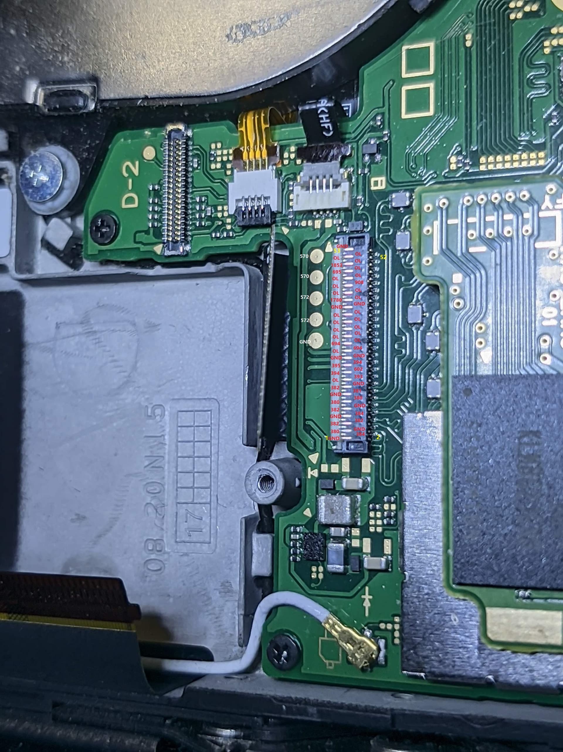
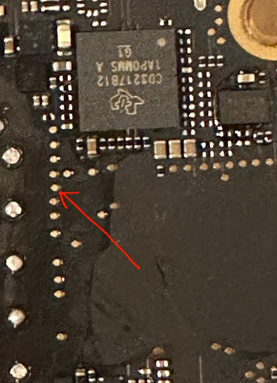
I have the following PCB, and I needed to solder some wires to the different pads, I had no issues with that, however, I barely touched one of the cables and the pad completly ripped off (I wanted to use uv solder mask after connecting all the wires, but I guess I should’ve done it one by one). How can I “recover” the pad? I see no traces and I cannot check for continuity to find another point where I may be able to attach the wire.
(note that the photo was taken before the pad got ripped, but the arrow indicates it)
Easy done if the TP isn’t either a stop gap (the TP being the go between) or the wires used being a bit too chunky, or if there is no via directly below it.
Bit hard to tell from your image but it looks like the tace or via is coming from the right, if you can show a clearer and closer image on the TP in question I can confrim, but if it’s a via on the right you may have to dig down a little depending on the damge to get to it and if it’s a trace you’ll have to scratch back at the mask with a blade to reveal it.
If it’s a VIA and if the concern is causing more damage to reveal it, you may be better off buzzing out where the VIA goes on whatever is left of the nub and soldering to that instead.
Is there a boardview for it? as from the image it just seems that the VIA’s only purpose is to take the connection to the TP (IE: serving no real purpose), if that’s the case then you can solder to another point where this line comes up (assuming there is another point) and the boardview would be able to confirm this. If no boardview is availiable you’d have to find the nub of the VIA and buzz out where it goes.
What is the issue your trying to solve on this board btw?