I do have a defect switch probably with a defective wifi chip - switch was booting, but no wifi / bluetooth.
I would like to replace the chip from a donor board, but I was not able to reball it properly and - surprise - it won’t work and now switch stops booting with the Nintendo Logo.
Are there any good tips how to reball such chips ? I have not seen a stencil for that, but I wonder how this can be done in a good way.
Maybe there is some reball experience with there chips with some tips ?
Just checked and have seen that I already have one - which is called BCM4354 (I should have seen it before)
Would suggest using solder paste with the stencil is the best way ?
Yeah these stencils are too thin to use prefromed balls in them (that is, unless you have a way to raise the stencil slightly higher in a uniform way)
Only thing really worth mentioning I think is, prior to using the stencil and solder paste, when your tinning the IC, don’t be running your soldering over it at a temp of over >320C for prolonged period, the kapton esq coating on this chip is particularly less prone to heat than other similar coated chips and you can just wreck it… If i remember right I typically tin the chip at about 250/280C prior to reballing.
I have had some tries with the stencil - but in the end is has not worked (yet) - maybe it is not a problem with the reballing than with the board itself.
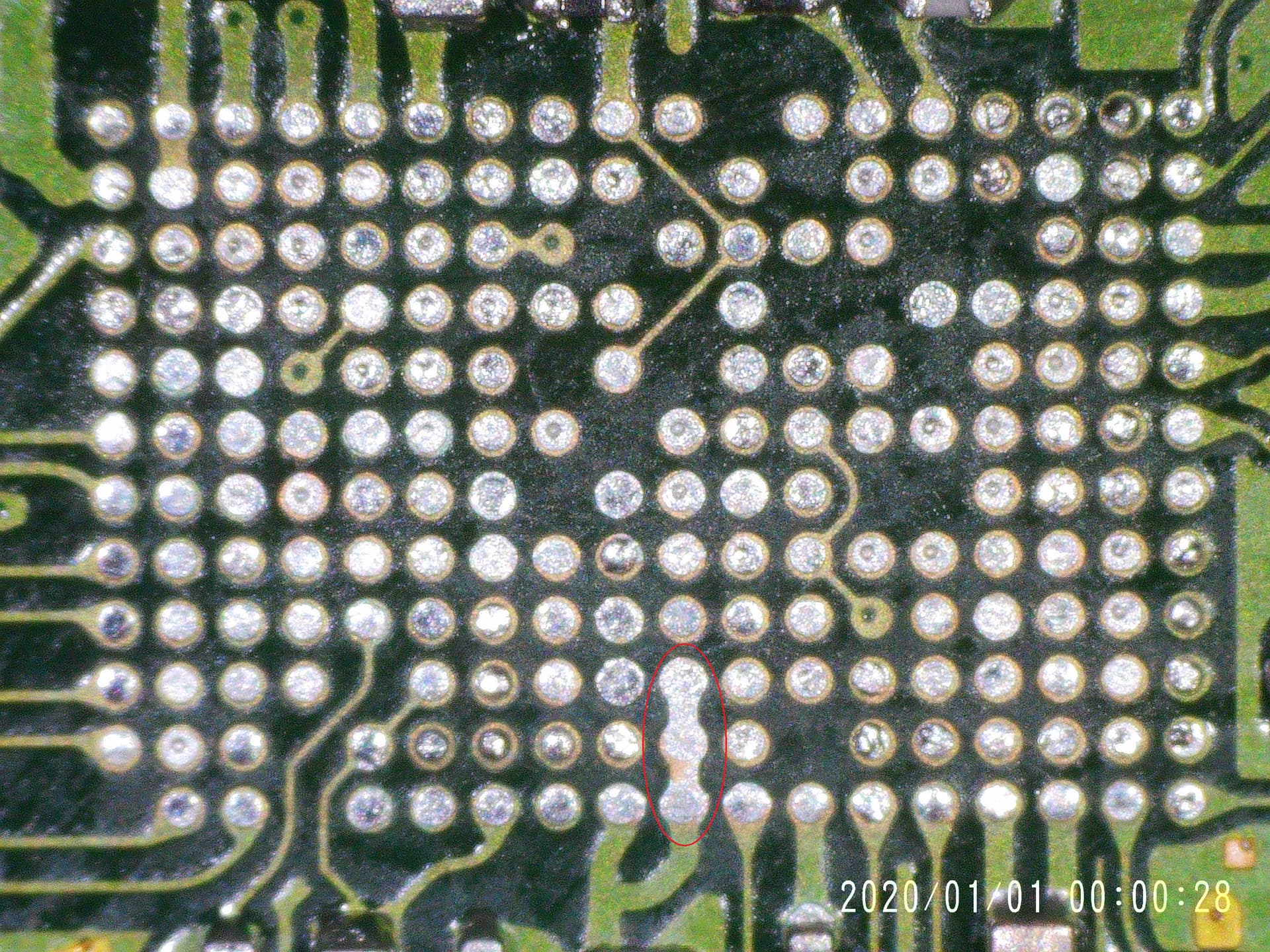
After a deep inspection of the WiFi area it looks, that I probably created a short. Looking at another board it looks like there is no connection for these 3 balls - but not sure.
I guess as long as these 3 solder points are not connected anyway it cannot be fixed - but not sure is this or if I must use it as a donor board?
Now the board hangs in the Nintendo
Logo Screen - maybe coming from this? Not sure if anything can be done here or if I have to use it as a donor ?
Theyr’e supposed to be joined, the only thing that might occur without the solder mask sepearating each indavidual pad is potentially pulling the chip a skew during reflow or the contiguous blob of solder sinking during reflow and (and I haven’t checked) if the opposing pads on the IC are not concurrently connected. thus causing a potential NC
It’s entirely possible though, that the fault lies at the SoC end (likely at some wifi/bt related connections) which may be the true underlying fault, as it doesn’t sound like the symptoms have changed between you replacing (I am assuming your using a “new” chip off a donor here) the IC
As an aside… Ask yourself how you would verify this on your other board using your multimeter
@Severence thank for that advice with the multimeter - I was a little bit ‘blind’ in that moment - any yes these 3 balls have a connection.
Before I gave up I just have reballed it again - and tried to be very accurate.
I also have seen that from previous attempts there was a very small solder ball (from the solder past) which was in that area and might have created a short.
Don’t know exactly but in the end, I was successful, and the switch is booting up again with WLAN now