Thanks man. For me I’d just be examining the voltage/s at the CPU/GPU reg, specifically at the output inductors and seeing what the behaviour is prior to boot, just battery connected then following this what happens to the voltage after prompting to boot and see if anything changes. I’d also be curious to know what happens on these outputs when the OLED is put into sleep/stanby and same deal over at the main PMIC.
One thing I would also look at is rail order at the main PMIC aswell as the CPU/GPU reg, backlight and LCD driver (this would be the 8316 IC on regular revs and you might be looking at their enables or PWM signals instead in the latter two cases instead of outputs) outputs etc etc on a scope or LA - I’d do all this to get an idea as to what the sequence is following prompt, this way you have a map - for example, missing 1V35 (typical on Mariko SoC boards) you could look at this map and see what comes prior and deduce - We already know the fuel gauge comes prior to 1V35 being enabled and can rule this out in Sheriffs case - the rest is pretty well unknown, I’m pretty sure the CPU/GPU reg needs identified prior on Mariko boards too. - The reason for this approach instead of specifically looking at IC’s on the I2C bus is I’ve had scenarios on Mariko boards where the failure is unrelated to anything I2C related although it could be like a feedback loop.
btw I’m not expecting you to do all this Coda, especially not in one sitting… I have a rough idea of how the original rev switch operates in this regard but the info was acquired in drips and drabs over several months. but this is what I’d do to help in Sheriffs case.
@SheriffBuck nice work so far man would it not be better to use your boot CPU rail as your trigger in this case? I know most things are going to be at a 1.8V or 3.3V LL but if your going to be examining further lines on your LA going forward there may be more to be revealed and I’m pretty sure this rail comes up first no? or I’m remembering wrong
Thanks for all your support and feedback. We’ll get this one cracked! It does feel like CCPLEX isn’t launching so agree it probably makes sense to focus around the buck and to make sure that everything measures out correctly.
One thing I could check this weekend is to block the CPU buck from providing power on my reference unit and to get a genuine picture of where BPMP finishes its work.
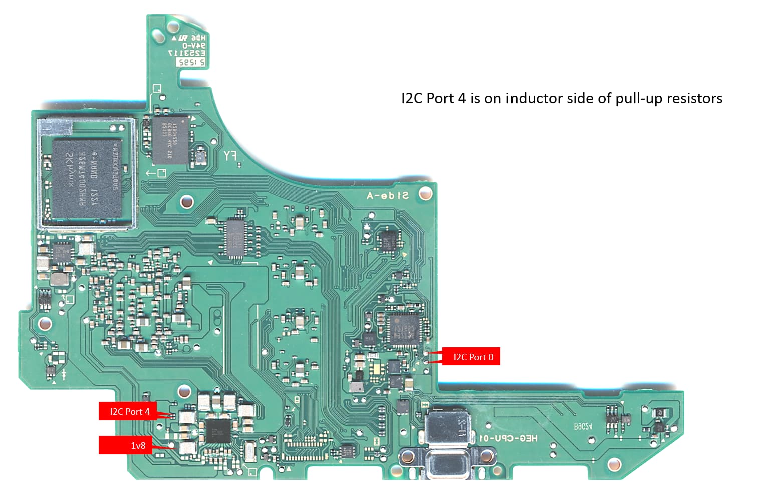
I’ve just double checked and the 1v8 rail comes up before the CPU Buck, so it made sense for me to consistently launch timing from that. I suspect the 3v3 rail is even earlier, but that creates problems for the LA.
I’ll follow up with a diagram of where I’m probing on the board.
Mmmm. I’m re-reading your question. BPMP CPU rail. I hadn’t appreciated the distinction as I’d always focused on CCPLEX CPU/GPU buck outputs. I’ll take a closer look at the TEGRA docs to see if I can trace that power feed.
No this is my fault. I tend to shy away from using terminology from any one IC as I’ve been stung doing this in this past with other devices - as in a lot of cases (though probably not in this specific case) naming conventions are shared on different IC’s but are completely unrelated to each other as a whole - for example I think the M92 terms “1V8PDR” as VDDIO but there are various other chips on Switch with I/O using this terminology/name which are completely unrelated which is why I’ll use these daft names instead
OK. Having delved into the X1 Technical Manual and done some cross-referencing to SwitchBrew, I believe the BPMP is powered by VDD_SOC/VDD_CORE which in the docs should be 1v125, but in practice seems to measure out at 1v15v. It’s provided by PMIC on the LXA/B_SD0 pins which all matches up. On the MAX77620, it’s the rail emerging from the bottom edge of the IC linked to two inductors. This layout seems identical on different revisions.
So I can take a reading from this rail for my trigger and see how that matches up with 1v8 which I’ve used up until now. I’ll also investigating blocking VDD_CPU which is provided by the MAX77812 on Mariko and see what that does to the boot flow.
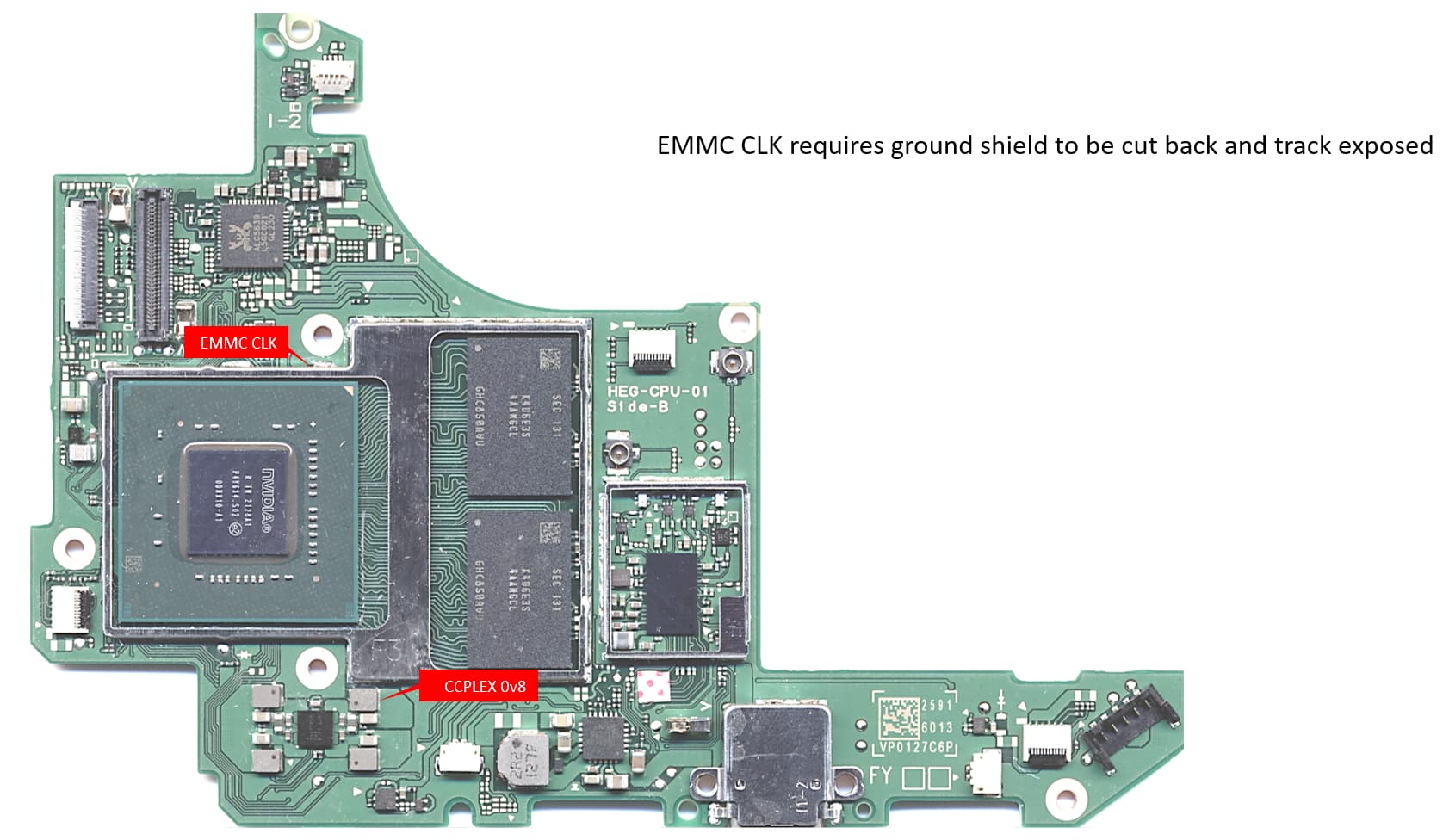
OK. Update from this weekend. I’ve checked the key contacts of the EMMC section of the board with the IC removed and everything checks out fine.
On my reference board, I removed the two large inductors from the CPU buck side of the MAX77812 and re-ran my tests. The problem with doing that is that the feedback loop on the MAX is broken and it’s power output goes unstable (the IC samples a couple of power pins on the Tegra in the middle layers) so this doesn’t seem to be a conclusive test.
When powering up the board, the boot stops after the first large block of EMMC clocking, then I see repeated, infinite attempts to negotiate with the MAX77812 on I2C. I’m not convinced that this has proven anything as boot appears to be stopped because of the I2C issue and not the lack of power on CCPLEX. Either way, the OLED gets further than this.
OK. More thoughts. I’m going to tombstone the inductors and put a resistive load in place to see if that can at least introduce some stability on the output side of LX3 and LX4 on the MAX77812.
The other thought I had was whether I could count the EMMC clock cycles / D0 access and calculate the data reads. I’m assuming both Package1 and Package2 are binary files that are fully read into memory in complete blocks, so we could get a definitive view on when they are loaded and then determine from Nvidia’s boot examples how this works… I understand that data is read on the clock rising and falling edges, so 1 complete clock cycle would be a byte of data from EMMC?
I do apologize, but I was unable to get any readings this weekend. The OLED i ended up working on turned out to be more of a horror show than anticipated. Looked like it was going to be just a standard port repair until i opened the thing…
Needless to say I was unable to get this particular board to boot and I did not have the time needed to take a second apart. If I find the time during the week Ill do what I can, but these days my hobby time is strictly on the weekend unfortunately.
Can I ask the reasoning behind doing this? Without the boot CPU rail the boot CPU can’t in effect run. If the boot CPU isn’t operating then not much of anything is going to happen afaik (which includes handing over to the other CPU). Is it just to see what other rails do and don’t come up without it present?
This is half the problem in that we don’t know what default behaviour / voltage is on OLED here. As you know on n a standard rev if the main CPU rail (CCPLEX) were coming up (and then after the GPU rail) you would be presented with at least the second boot logo. If the same rules apply here it does indicate or imply that the main CPU and GPU is not operating regardless of the voltages measured at the CPU/GPU regulator, that combined with missing 1V35 suggests it’s halted somewhere pretty early in the boot process. As an aside, didn’t we figure out what 1V35 was actually for ages ago Sheriff? I’ve got no memory of what it’s purpose was
Sorry I’m not familiar with the EMMC protocol or even if being in single bit mode would alter this. My thoughts were it’d be a bit per dat line but I’m probably wrong
So the MAX77812 drives CCPLEX and the GPU, however it doesn’t drive the BPMP (boot CPU). I was trying to determine what stage boot gets to on my timings on my reference unit. That way I could determine whether the OLED is progressing to CCPLEX on the execution chain. By pulling the power to the CCPLEX, I’d expect boot to fail at the point where handover occurred. Hope that makes sense!
I can take some measurements on the 1v35 line and the timing on Mariko in relation to boot. Looking at the Switchbrew notes, I believe 1v35 feeds LDO0, LDO1, LDO7 and LDO8 which are Panel, Xusb, PCIE.
Been working on this some more today. Contrary to what I previously thought (due to some dodgy annotated diagrams I had been using from online), the Switch has an 8bit EMMC data bus and is capable of running data reads on the rising edge only, or using DDR (which is rising and falling edges). That means for every EMMC clock cycle, the system can pull in a byte or 2 bytes of data.
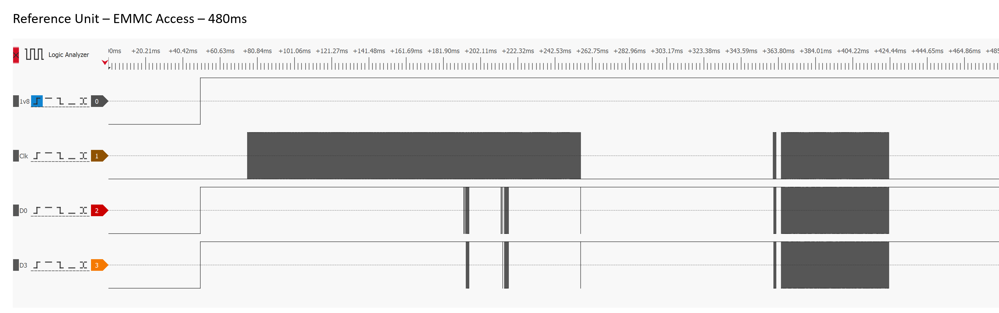
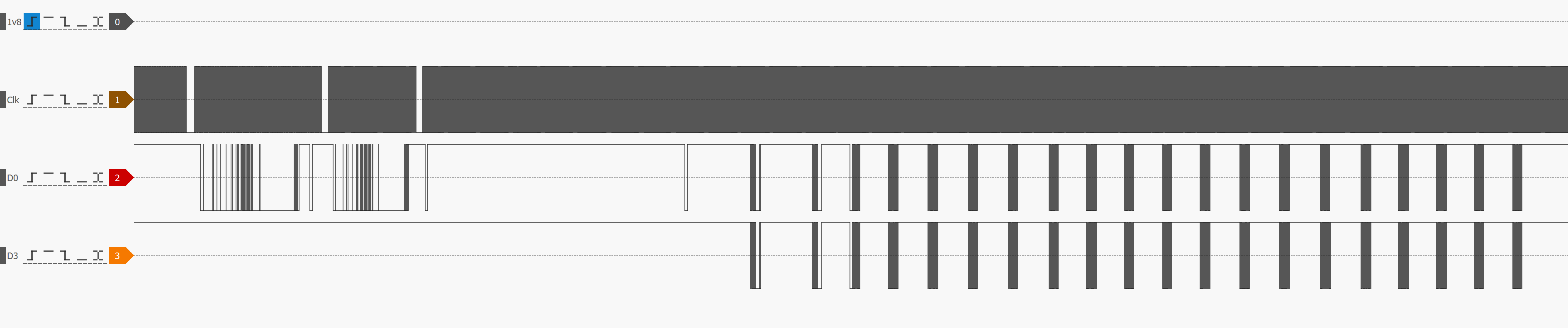
So update from today with my reference unit and investigating EMMC activity. The boot process starting from the embedded CPU boot ROM (Nvidia) which reads the 16KB BCT from EMMC. Once ingested, it then jumps to a preset location and reads in Package1 which is 256KB. Finally it moves on to read Package2 which is roughly 2.8MB.
By counting clock cycles, I believe the first EMMC data transfer (at 190ms) is the BCT read closely followed by Package1. Package1 executes and as part of its execution, reads Package2 into memory (210ms), this time using DDR. Once Package1 completes its execution path, CCPLEX is prepared and execution launched of the Package2 payload in memory.
So I believe the large block from 350ms is Package2 reading in more resources from the system partition as it begins to assembly Horizon in memory and boot from it.
Looking at my OLED data captures (which admittedly only have the EMMC clock at the moment, no D0), it would appear that the OLED is comfortably executing Package2 on CCPLEX. I’ll try and test the theory with my work on the MAX77812 mentioned earlier.
This seems to suggest that the OLED is getting to CCPLEX boot stages but is failing somewhere along that.
Sorry, ignore me, I’m an idiot, I completely misread your previous post and thought you were isolating the the boot CPU rail via the two inductors (those pesky Max IC names)
Interesting. So if I understand correctly, that’s a bit per dat line, 0 to 7, making an 8-bit byte, x2 = 2 bytes? what about at boot when it’s presumably starts in single bit mode initially, or is data always read off the EMMC exclusively in 8-bit mode?
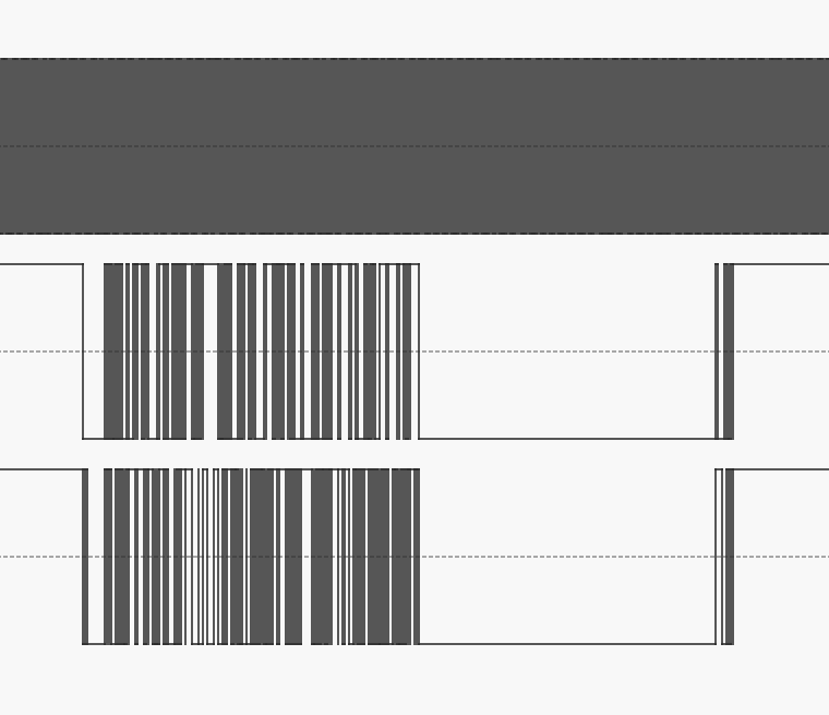
So we can see the early stages of comms, it’s all 1bit mode. Only D0 line rings as the early stage handshaking and CSL registers are read. It then ramps up to 8bit mode immediately. It seems when the handover happens with CCPLEX, it re-initialises control of the EMMC (after all it’s a totally different core), and it starts it’s 8bit handshaking all over again.
You can see it really clearly when you zoom in. 1bit handshaking on D0, then ramps up and each of those blocks I think is 64kb of data chunked out of EMMC and into RAM. That’s Package1 being read. Beautiful.
This one I think is the BCT read and it does it twice. It’s quite obvious when you look at the structures on SwitchBrew and you see that a large part of it is padding.
Dear Sir,
My Switch OLED is suffering from the same issue as yours. Have you fixed yours? If so, could you kindly let me know what the issue was?
Thanks a lot.