Hi all,
I managed to repair some Nintendo Switches - thanks to you guys and the information here in this forum.
A few weeks ago I got a Switch which had a blown pi3usb and two ripped pads. I soldered jumper wires and replaced pi3. Everything seemed to work for a few days and all of a sudden the Switch didn’t power on anymore. I then replaced the orginal usb port and the switch started powering on again.
However whenever I place the switch into the dock or plug the 15V charge cable into the switch, the switch shows the error code 2101-0001 and prompts to reboot. This does not happen with a 5V charger. Today i replaced the pi3usb again and also M92 but still the same behaviour. Also the CPU gets quite warm (in compare to other Switches) when powered on.
I checked some of Calvins diode map readings and could not find anything obvious as well as no shorts around the usual ICs.
I can provide some pictures if needed.
Do you guys have any ideas on what to further check? Thanks in advance!
I have measured in diode mode 0.770V for D+ and 0.772V for D- (at testpoints above usb-c) as well as contiuity given to the corresponding usb-c pins. Any other ideas?
Hm I already replaced the M92 once and still the same behaviour. I also checked the pins of the new M92 and compared with @Calvin Diode map - every pin seems to have the correct diode mode value.
Do you really think another replacement will help?
I will try and post some images of PI3, M92 and the port area later.
@Severence Sorry for the delay… had a busy work schedule
I have already replaced 2xPI3USB, 1x Port, 1xM92. Also when i put the Switch into my Dock today, my Dock died (I think the Dock Charge IC was fried)… This is really weird. What could cause such an issue with 15 V? Could it be a false M92T batch or my bad soldering skills ?
I can take further measurements and post them here if you want. Thankful for any further hints.
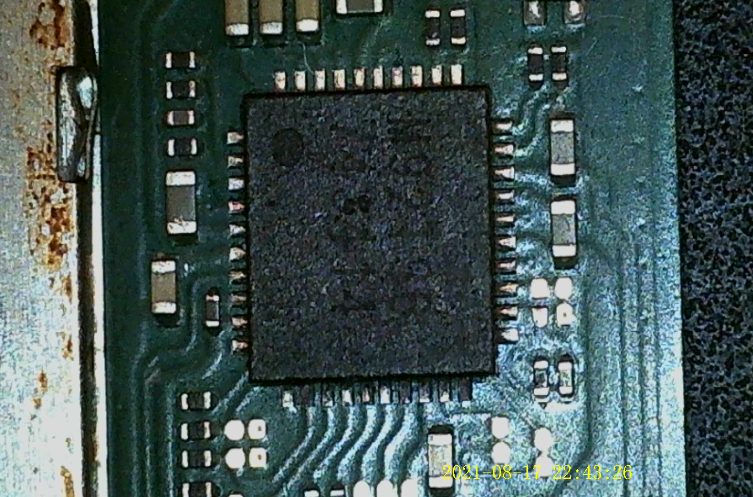
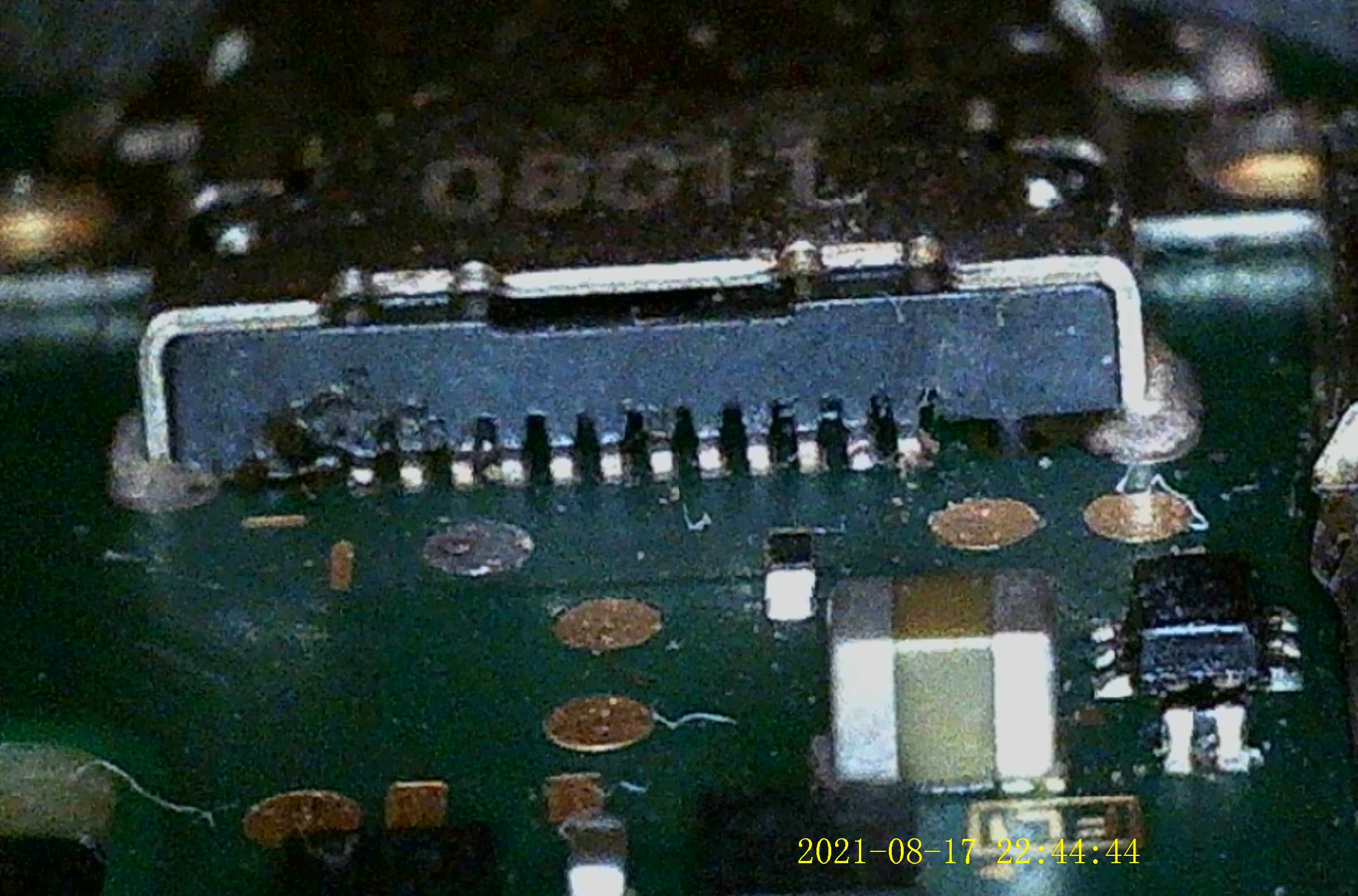
I may be wrong, but is that a bridge between the USB pins 3rd and 4th on the left of the pic? Also, I’m not convinced the USB port is all the way flat, the right side looks lifted a bit.
Don’t think the primary issue is of flatness (think it’s just the camera angle), I agree with insomniac that the issue at hand is a bridge across pins, looks like the inner row to me…
You can check this by seeing if you have continuity across pins/breakout (or filters) where you shouldn’t - this would explain why you killed your dock.
Some of the joints on ICs perhaps look a little anemic but other than that should be fine
Hm - I didn’t find any bridges when testing at filters/pins according to the usb c Diagramm for the switch. I will change the port regardless and post my results. Keep you updated and thanks for your hints.
So it was not the port, I placed a new one and checked the outer and inner rows for the correct diode values as well as connections to the board… I could try and replace M92 and/or PI3 IC again but i doubt that would help. Running out of ideas…
Well if anything, at least your USB looks like a cleaner install now
Whats your resistance to ground on 3V3PDR?
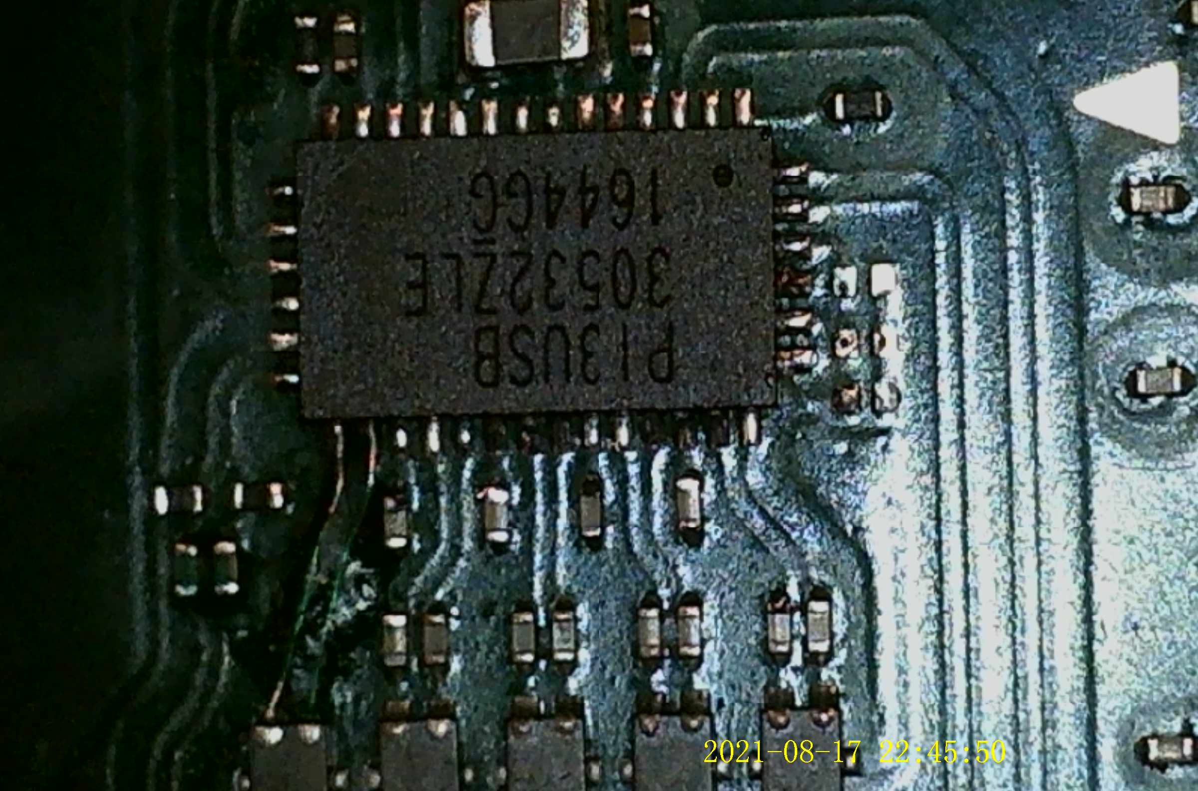
Instead of taking diode mode readings, check continuity from the USB to all relevant points and the same all the way back to the P13, don’t check at the P13 board pads but instead the IC “pins” round the edge itself
As in the little rectangular pads on the IC itself around the edge, it just verifys that all IC contacts are in contact with the board if for example your P13 wan’t down properly youd see if with lack of continuity
Ok, just to make sure I understood your thoughts:
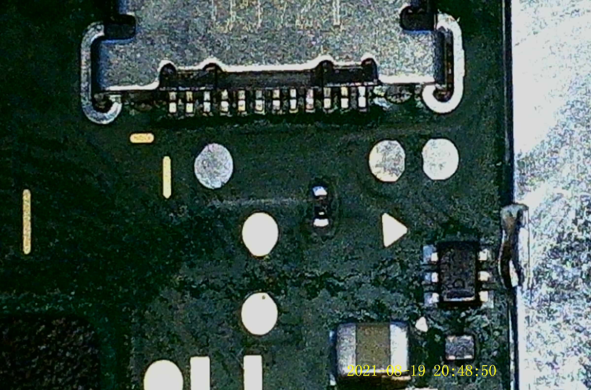
So you suggest to take measurements at the pink circle highlighted pads instead of the board Pads (green Circle)?
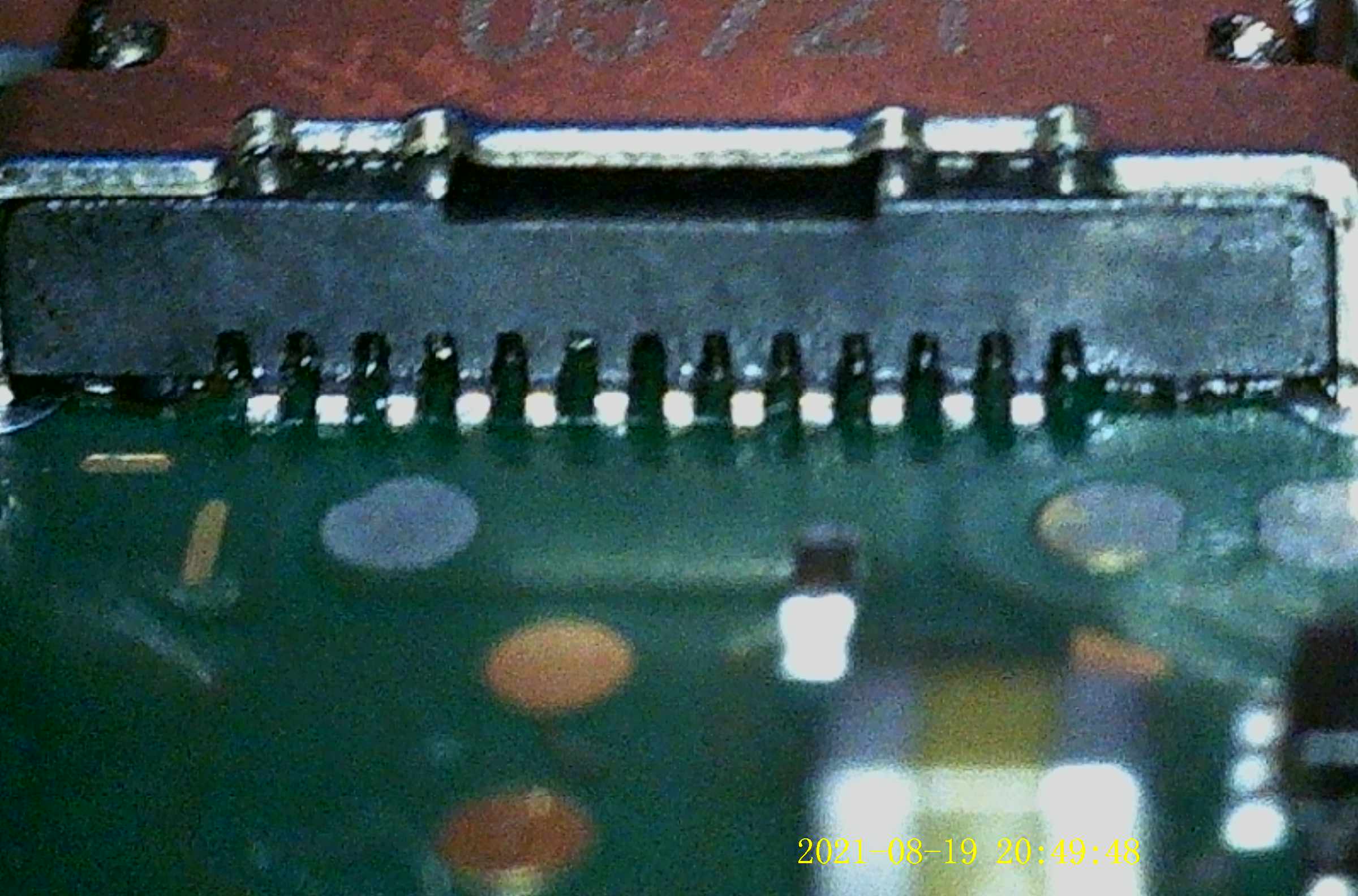
Hmm it looked like some pins of PI13 didn’t make full contact with the ic pad itself. I replaced PI13 again yesterday but now the switch does not turn on anymore (draws 5V at 0.44 A). There’s still some pins missing the full contact to the ic pad. I will resume the repair in 3 weeks when I‘m back at home.
Can anyone give some tips on how to form a nice solid solder joint from the board pads up to the „ic pad“?
Tin the pads with leaded solder to lower the required temperature. Try to avoid lead solder in the center ground pad. You can tin the legs of the p13usb IC for better connection. Then you can run a d24 chisel or a JL tip to touch up joints. At the end, you can check with a diode map to verify all the connection are done properly .

 ?
?

 (draws 5V at 0.44 A). There’s still some pins missing the full contact to the ic pad. I will resume the repair in 3 weeks when I‘m back at home.