Recently I got one switch V2 (Mariko) that had botched picofly installation. To not go into much details, it had black screen, only backlight would turn on. I removed all of wires and cleaned it up (it even lost SP2 capacitor, left pad was lifted…) and it turned on.
It looks to be functional, works fine (left it looping in some demo game for 30ish minutes, no problems).
But I noticed that touch screen doesn’t work. I checked cartridge daughterboard, looked fine, no soldering on it, no scratches. Doesn’t look like it was moved or touched, plugged in the mainboard OK, touch ribbon also doesn’t look like it was damaged.
Yesterday I got one switch with blue screen (probably beyond repair, it’s bent in the middle as if somebody sat on it, even motherboard was a bit bent when I took it out, although oddly enough screen didn’t crack…).
I tried using it’s daughterboard, it also looks to be fine, no scratches or bends, but there was no change.
check the blue screen one has same type digitizer that your v2 picofly one has or not.
There are 2 types of digitizer, one has QR code on touch ribbon, the other just few characters no QR. The daughter board module has Touch IC(FT9CJ) programmed independently for type of digitizer.
Or do the Hekate touch calibration if possible
Do you know if they can be reprogrammed / have you done it? saw mention of the lines etc on the recent JC topic, on the Git page, so just curious as I’ve developed quite a collection of these now which don’t work with the digitizers I’ve got
The IC should be able to reprogrammed IMO but not sure how.( cause replace another type digitizer is cheap and easy enough for me).
I saw the clone type daughter board has Chinese combined rectangle CHIP (instead of FT9CJ square) that works both digitizers, price wise is pretty much same as refurb/original daughter board.
Wow, thanks for replies, didn’t expect anything so soon .
Here are both ribbon cables, just my luck, they’re different, bent one (upper one on the image) has QR code on the cable… (can’t upload or embed link so “raw” link…)
https://i.ibb.co/mNznqz5/Ribbons.jpg
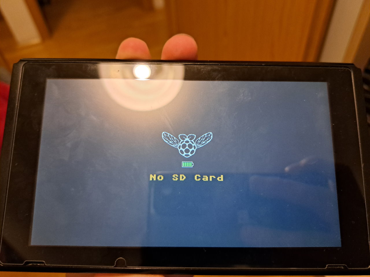
Unfortunately this one is not modded so no hekate.
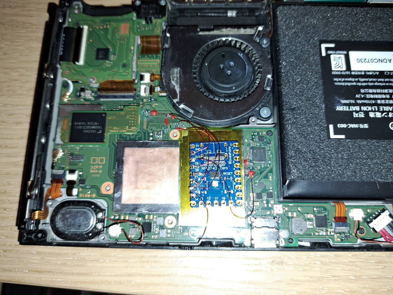
I tried redoing wires, there were not shorts, connections were OK going to picofly (rp2040-zero) but I only got “emmc init failure” code from picofly and it booted to OFW.
I tried to swap one soldered with my own picofly, just to test if there’s something wrong with it, but same thing happened. Tried with 2.73 and 2.67 firmware versions, just to test, but no change. Only boots to OFW.
Ribbon cable could only be soldered to SP1 on APU since SP2 point pad is lifted. Maybe this is the problem? I might try getting RP2040-NS board from aliexpress to try again…
In reference to my deleted post above: I was going to say have you verified the patient EMMC on your other modded, but I suppose that’s irrelevant as your patient is booting OFW which mutes the EMMC being at fault
Quite possibly, should be able to pick up the VIA nub and tack to that, of find an alt point (which there are many) and solder to that instead.
Can you clarify this. This is a second Switch console, right? and this one has a bend & BSOD? and when you say it has a bend in the middle are you reffering to the assembly or the board, or both? (very recent topic here on the forum regarding ram / bent case which might be relevant here, so might be worth finding it) , anyway, so let’s call this Switch #2 . If I understand you right, your tried the GC PCB from this one on Switch #1 and the touch issues remained the same?
Unfortunately yes, everything works, except picofly. Actually, it also works, just not for glitching .
I tried scraping substrate a bit, but it’s tricky. pad was small already, and there seem to be ground plane around it and it looks like there’s only tiny bit of trace that was connected to the pad. I’ve covered ground plane with solder mask and tried to add solder to that tiny bit of trace to replace missing capacitor but solder won’t stick to that tiny trace…
There are alternative point for SP1 and SP2?
Yes, #1 is botched picofly install, #2 is BSOD and bent switch. Both are bent by few degrees. With case being worse. Bend is cca along the battery compartment, so only lower lip of the board is bent slightly. There are no obvious cracks there so I might try reflowing APU and RAM with hot air. Maybe it’ll revive.
Yes, I tried using GC board from this switch but there was no change. But digitizers are different so that might be the reason…
yep loads, you can buzz out the locations on your other board in continuity (I’m purposely not telling you the answer here as it’s good to learn how to do stuff for yourself… ask yourself how others know this stuff )
I see.
SoC reflow should absolutely be a last resort.
Ram reflow is a viable option (assuming of course this is a Ram related issue and that the bend was not so severe that it ripped the pads or traces off below)… provided this is to be your own personal console, I can’t endorse it if your planning on selling though due to the nature of fault (bend) and the high likelihood of the problem returning… Find the other recent topic regarding Ram and reflowing for guidance and how to narrow down (again, sorry, I’m not going tto find the info for you or spend an hour typing the same stuff I’ve typed up many times before )
Odd, you’d think it would given the two different types of digitizers they are paired with, unless either of the sellers have mixed and matched parts. Do you get any sort of touch detection on Switch #1 ? (either of the GC PCB’s) usually you’ll get touch detection around the edge of the digi (in regard to one of these FW / calibration mismatches)
I’ve already googled about this but haven’t found any mention of alternate points for SP2/SP1. Especially since they’re not on motherboard but on APU. If right pad was missing I wouldn’t worry, since that one is GND, I’ve already checked that with multimeter.
And the other one is bent one with BSOD, which could mean broken soldering under APU or even broken traces somewhere in PCB layers. Using it to trace would be like looking for a needle in haystack, with needle not necessarily being there .
Whatever it may be it doesn’t work. I tried pushing APU and turning it on, which helps when there’s APU solder problem, but it didn’t help. Heck, APU didn’t even get warm. ¸
I think that switch is pretty much dead, or donor. Reflowing RAM and APU would in the “let’s see what this button do” basket. Making keyring from that APU is also not out of the question .
I don’t sell things (picofly one was just “can you fix it please!!!”), bent one I bought cheaply to see if I could do something. That’s why I have a lot of vintage c*ap . If by some kind of miracle it revives It’ll go in my collection.
Like these things are which I also got dead, but managed to revive (and upgrade with modern screens after ). These are just part of collection
But that’s moot point, topic of this thread is touchscreen on picofly borked switch, not this BSOD one.
I have my doubt about BSOD one, description was it was dropped and since then it has BSOD… When it arrived it turned out it’s bent and there were screws missing. So it was opened at least once. Who knows what else happened there…
I even tried using BSOD GC board connected to borked picofly motherboard and BSOD digitizer and it didn’t work. Maybe that digitizer is also borked, although there are no cracks in it and LCD underneath it also isn’t cracked.
If I manage do install new picofly to borked one to get hekate to run we’ll see.
Yes this is what I’m talking about, talking purely about the “signal side” of the cap/s (which is the only side we are interested in) instead of using google, put your meter in continuity and buzz out the alt points with your meter on another board (again, ask yourself how others work this stuff out and/or verify if the point in question is getting from one place to another) This is basic, basic stuff bud, I have faith in you
Right, is largely irrelevant in this situation if that were the case. (provided ground is connected elsewhere… albeit with some caveats)
Emphasis on the “could” part. As mentioned could just as likely (or I should say more likely) be RAM, could be ****SoC **** , it could be Fuel gauge, could be EMMC or could be PMIC. If you try to reflow the SoC, in all likelihood without exploring the other avenues I mentioned then you are almost certainly guaranteed to kill the SoC and thus the entire board as a whole.
There are methods of detecting OL/ partially open lines, you can sometimes get a good indication by measuring the IC’s primary rail/s in question relative to ground (sometimes both polarities) to get an idea.
Speaking for myself, I’d have pulled the ram off the board (after verifying fuel gauge) straight off the bat, then inspected the traces / pads, if problem seen, repair conducted etc, ram reballed etc etc, failing that (no trace damage) only then would I start looking elsewhere for a potential fault (again SoC would be last on my list) Not that I’m saying you should take my approach if your a beginner.
Again, recent topic I mentioned (clue it was at least within the last 20 Switch related topics) delved into this, and what you should actually be doing instead of what you are doing and what potential impact bad ram / bad ram connection could have on other aspects of the board.
Haha, not a bad Idea
Sweet collection dude!
Ahh this changes things, Fuel gauge and EMMC go up a rank in terms of suspects. (bent case would still need to be addressed later if that is the problem and it’s resolved.
Right, but in either case, did the digitizer work around the edges (this is the typical behaviour) ?
It’s actually easier to solder one mosfet to this capacitor than it is to solder flex cable on CPU.
And I don’t know if it’s placebo or not but I have a feeling that glitching works faster on this setup than on flex cable version.
I have one modded with aliexpress picofly-hwfly clone and that one takes few tries (blinks) to glitch. While this one is in 90% percent of tries instant.
As for touch still no go. It doesn’t work on edges, and when I try to recalibrate it through hekate I get “Touchscreen calibration failed” on both card reader PCBs I have.
Unfortunately I don’t have any cartridges to test if anything on PCB actually works.
I’ll have to probe to see where power goes to that PCB and see if there’s some power issue there. Since I get same “failed” message when I try to recalibrate touch when cart daughterboard is not even connected so it smells like there some kind of power issue to daughterboard .
Seems like a hardware issue. One of the reasons why I wanted you to figure out the alt locations for modchip install yourself earlier was because it would give you the knowledge to potentially diagnose and fix your GC PCBs (boards are very thin and VIA damage is common on them) , also the reason why I wanted you to attempt to solve your other board issue is because it’s also possible you have an issue mainboard side which you’d be able to rule out with your other motherboard.
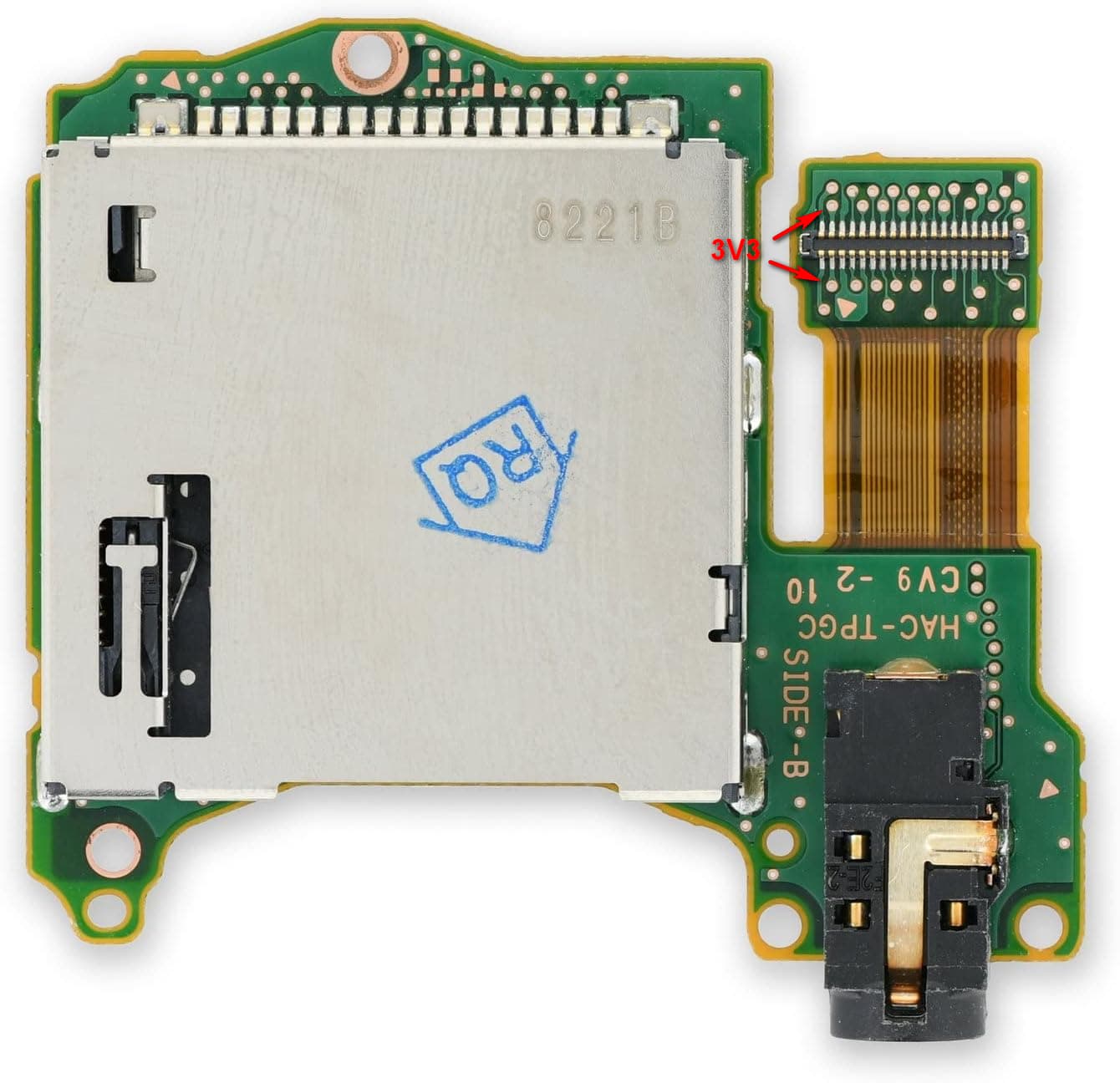
Also, another thing worth checking is, the connector from the GC PCB which attaches to the mainboard, often times it curls / bends and won’t make proper contact (usually from people trying to mash it in wrong) so you sometimes have to bend it back straight / true.
Connectors look OK on both daughterboards. I always gently push them until they snap into their socket. There wasn’t any feel of resistance, when it was positioned correctly it just snapped in.
That’s why power is the next thing to try. GND is OK, there is connection. I just need to find power line and see if it’s ok, and if it is try with switch powered on to check the voltage there…
Time and space are the issue. Although not in SciFi sense .
I dont’ have work area as I live in an apartment so I don’t have much space. During the week I can’t tinker with electronics as the desk is used by my GF because she works from home. Only during the weekend I can clear it to bring out the tools, and it’s not exactly like I can spend whole day probing .
That’s why I looked for solutions. I can do some repairs, but to probe points would take weeks .
For some solder points I used http://balika011.hu/switch/erista/ to trace paths along the layers and narrow the search (capacitor that’s used for powering picofly was also pretty damaged so i looked where else that rail goes).
Instead of checking for voltage (and this ties back to what I was talking about earlier) you’d be better off doing a visual of the PCB and looking at the VIAs on the GC PCB (particularly those closest to the all black connector) and looking for any signs of damage / corrosion and then testing continuity for opens etc
Haha, yeah, I hear ya
yeah, it’s a good resource but, don’t forget you’vre got another board and often times it’s quicker (sometimes clearer and more obvious) to just buzz stuff out (tip: you can strip some heavy gauge wire and connect to to your meter and then use the wire like a paintbrush, then you can find points in continuity extra extra quick) . You could get youself into trouble relying soley on that site as sometimes it can be misleading, as the alignment beteen layers isn’t 100%
Plugged it in, turned it on and 0V on these points. After that I unplugged it (after I disconnected battery of course), and turned it back on to check voltage on connector pins and again 0V.
But I probed other vias while PCB is connected and found multiple 1.8V and one 2.8V spots so who knows. Maybe there’s no 3V3 there until there’s game inserted.
I think it’s better not to mess stuff that works , at least until I can find some schematics.
Right, so next you’d wanna check that this is the same rail as 3V3PDR or not by checking it has continuity to one of it’s locations on a known good (at M92 or PI3 etc etc) . Note though, that this rail only comes up following prompt to boot, so ensure when your checking the voltage on your patient that the unit is prompted either via USB or PWR button,
After that your can start narrowing things down
Doesn’t really tell you much, a lot of these are signal lines to/from the IC on that PCB