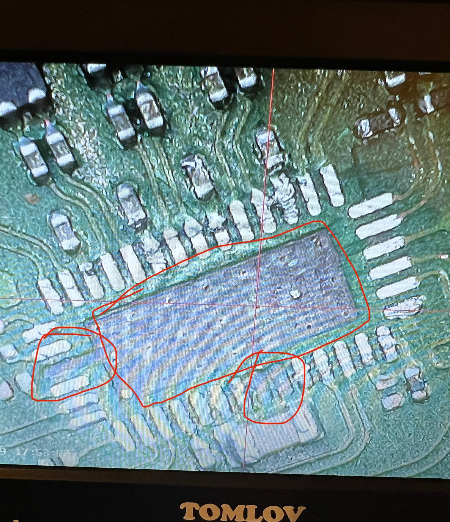
The video chip was fried to point it got melted to the board and that’s how it came off. Both boards I posted came from my friend don’t mind me I’m learning and asking for help for anyone knowing how to fix this or if it’s repairable. It’s missing 3 connections and whole base pad. Many thanks
The missing pin-pads at the pi3usb ic doesn’t matter. Pins 5,6 (DP2) and 8,9 (DP3) (<-Your missing pair) are n.c. because the Switch only uses DP0 and DP1 lines. And Your missing pad @ pin 37 is GND.
So the only thing to worry would be the big centre GND pad.
I would tin the centre pad at the ic and the both vias on the board and during hotair soldering, I would press the ic down till the tin becomes solid again after removing the heat.
1 Like
So you saying I don’t need to worry about those 3 missing links just that I need to reattach the pad back and using hot air to put it back with new chip? If so then it’s easy fix. I’m sorry if I’m a bit slow on understanding I’m trying to learn so thank you a lot for explanation 
Normaly you would have a big ground pad on the board and the matching pad on the ic. Now the big ground pad is missing on the board and the leftovers are the both vias.
You can try to rebuild the missing ground pad, but in the end you will connect something (whatever you use for replacement) to both vias, so it is easier to put a bit tin on both vias (check if they are making connection to gnd) and then solder the ic back in place and with this direct on to the vias.
The last 37 pads should give enough footing for the ic.
Just as a side note, regardless of if the IC was “melted” a failure in this manner would not result in those pins/pads welding to the board… and in particular neither the center ground pad… what’s more likely is you or someone else pulled it too soon or too aggressively (maybe your hot air station is not up to the task), as such I would not be surprised if you have further via damage, I would carefully check from a USB breakout the lines going to and from the P13 in resistance, if any are high or open then you can assume further damage at other lines/vias through the boards inner layers and reserve this board as a donor
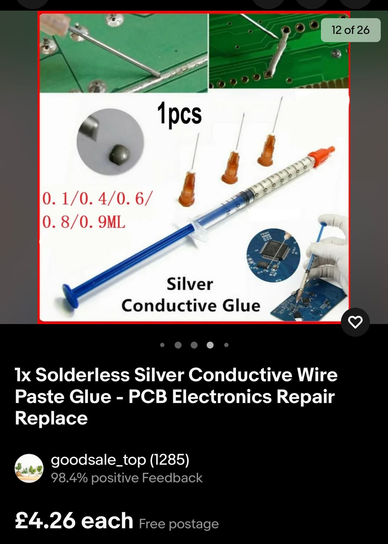
this stuff is pretty hopeless tbh, at best it should be used for repair of keyboards and the like (the carbon/silver traces on thin film plastics) but even then it’s pretty bad, some metal compound (I doubt it’s silver) mixed with PVA, it never truly dries hard and is always spongy, you can’t solder to it, it has terrible resistance/losses, just avoid this stuff. For pad repair get thte BST pad strips, the thicker versions
1 Like
Thanks mate, yeah most likely my hot air is trash I ordered new one with the preheating table. Most likely my fault  thanks for the pad replacement alternative:muscle:
Could you please share with a link as to how those BST pad strips looks like as just trying to google that doesn’t give an actual view of them. Thanks
1 Like
For the central ground pad I’d use something like this
and cut that manually to approx 80% of the dimensions of the missing pad, scratch back the through vias (you can see the the circles which are the vias) until you see copper, tin them with solder, then attach your cut piece of copper to that and press down with your iron, after seal the outside with UV solder mask. As for the thickness of the copper sheet, grab a few rolls and use your better judgement when they show up.
For the regular pads, the BST brand of solder pads are best, though double check the thickness, there are two variants afar, one lot is thin and the other is thick (they both look identical) you want the thicker ones so search around.
I’ll provide a link if I can at some point to the ones I got specifically… but having issues getting into my Ali account…
As I mentioned though, verify the USB to P13 lines first though using a breakout board and ensure none of your continuous lines are high or open before bothering to repair the P13 damage, and also verify the console actually even still boots too (P13 not required)
it’s amazing you actually managed to remove the middle pad without more damage to the pins.
as someone said the switch still boots without one, so I’d check that first.
I haven’t seen that pad missing before. but I have seen bubbling/delamination around the area due to to much heat. so I’d definitely see if it still boots.
Thanks all for the advices and suggestions, managed to get the P13 chip on after I soldered it the wrong way  switch works perfectly, took a while to get normal tools and actually sit down to fix it