I received one unpatched cpu-10 switch came with no power/no boot.
prob around found M92T36 area has cap shorts, thought was just common failure, replace new one, test with charged battery, turns on, 2nd logo come slower than normal,then shows up 2101-001 error.
Okay, maybe I just bad luck today, redo m92t36 with another new one, same.
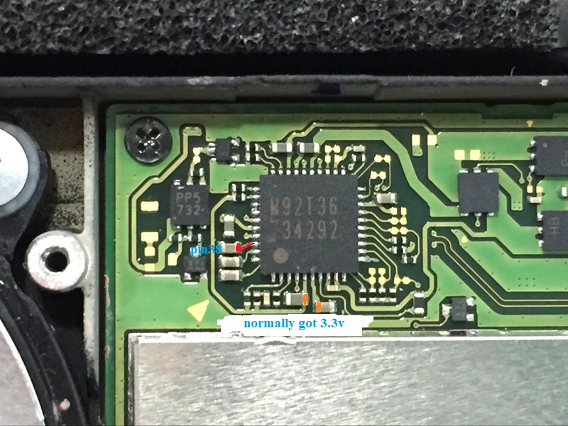
Weird, checked around and find that first-time charge cable plugin makes 15v0.7A then never goes back 15v,stucked 5v. More frankly M92T36 pin38 goes short after error shows.After that I totally tried 3times M92t36. All go bad after first boot.
Something I have noticed that, pin5,6 normally has 3.3v but 2.9v-ish after M92T36 goes bad(pin38 short)
Never seen any single board acts like this before, I first doubt was my m92t36 batches bad, but after 3times same symptoms, I highly doubt was max77620 or some other prior power rail circuit causing this.
change M92T36 with a new one. There are often bad lots
I have been using that lots/batch many times, don’t think that’s the case
just using same batch M92T new ic on another device replacement, works fine as usual, doubt this board was other issue causing m92t dies that quick
check your psu, then check 15v boost circuit
I have the same issue. I had a working Switch and after measurments at the sd card with multiple times re- and inserting a sd card it shows the error 2101-0001 and wants to reboot. The same cap above the m92t36 is shorted and I ended up in the same situation after replacing the m92t26 with a brand new one and restart the Switch, the before good measured cap after soldering is short again.
what is your resistance to ground on the m9 input 5/6 (forget which is the input off the top of my head), and also resistance to ground on 1v8, both polarities please.
Also sometimes when the surrounding fets fail or start to fail they pull certain lines low on m9 causing the failure. Also check resitance between USB pins (particularly on any any areas where there is charring on the plastic…if there is any)
Pin 5 at the m92t36 gave me (black probe on gnd) 21 kOhms and (red probe on gnd) 150 kOhms.
Which 1v8 circuit do you mean?
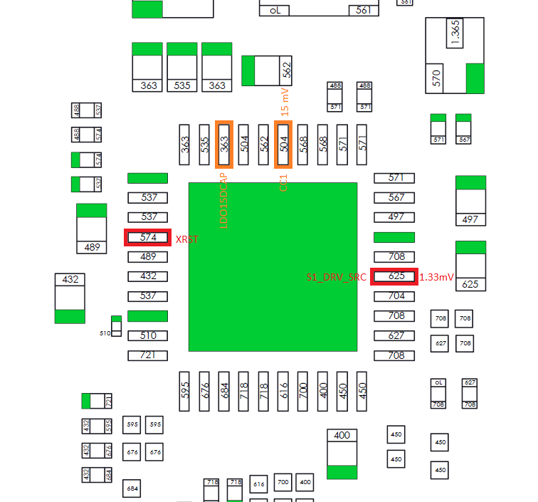
I found more issues on the m92t36:
cc1 is also close to short and xrst and s1_drv_src have aprox double voltages they should have in diode mode.
Sorry should be pin 6 not pin 5, pin 6 is primary 3.3/3.4v input supplied by “enc” ic below audio ic, dc to dc converter, the SD is supplied 3v3 and 1v8 which is why i’m asking about this.
My pin 5, black on ground 21k (or 100k if junctions triggered) reversed is charging megs (normal)
My pin 6 black on ground 16.6k and reversed is approx 150k
1v8 is supplied by max pmic and can be found at the following location
interesting, will investigate
Ok. Thank you.
At pin 6 (VSVR) black on ground 16.8 kOhms and reversed 150 kOhms. Seems to be the same.
At pin 18 (VDDIO) black on ground 5.5 kOhms and reversed 6.8 kOhms.
no worries,
Yeah, something is affecting this rail, should measure approx 10k/13k respectively…
Let me have a think on it based on your previous measurements
your measurments are almost the exact same as the correct readings but divided by two
This would seem to indicate a bridge/join or semi failure on something, presumably on the 1v8 rail
will mull it over
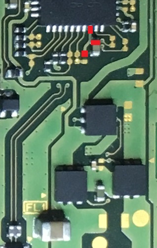
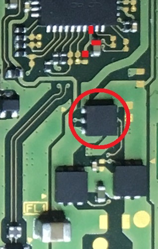
After a bit of thought…I’d remove or replace the highlighted fet in the image and retake the measurements you took above, also check the two fets below as they are all interconnected.
If the readings don’t come good, remove m92 and the fets and see if resistance measurements on 1V8 return to normal.
If the Values don’t change after removal, i’ll need to have another think 
I replaced the fet (M6/K03) and de- and resoldered the m92t36. Now I have instead of 1.33 mV --> 0.620 mV at pin 25 S1_DRV_SRC. Nothing else changed. XRST still has 1.33 mV and the shorts at LDO15 and CC1 and the resistance values pin 18 VDDIO at are still the same.
The resistance values were the same at the time the m92t36 was out.
Have you reworked anything else on this board, or are there any indicators of prior rework elsewhere?
There are so many crtical components on the 1V8 rail it’s pretty hard to determine what could be causing the dragged down reading but i will say it’s typically the soc ![]() but, in your case as the readings are almost /2 normal resistance measurments, it does point to something else potentially.
but, in your case as the readings are almost /2 normal resistance measurments, it does point to something else potentially.
This would again point to a joined pin/pad somewhere or a shorted transistor/fet (maybe)
Do the other fets sourrounding M9 test fine including the one above (resistance) ? and was the fet the cause of the original bad readings on S1_DRV_SRC or the soldering on m9?
Also LDO15 appears to be generated internally on m9, short should disappear with m9 removed
*Also LDO15 appears to be generated internally on m9, short should disappear with m9 removed, if not then it must be the *reference cap…at least when looking at the datasheet
I bought this Switch as defect but in very good condition. No signs of case opening or prior repair attempt. The M92T36 had a short (don t remember which pin (40/39/38) and one of the JoyCon rails had corrosion. I replaced the M92T36 and the JoyCon rail. It worked fine except there was no JoyCon plug animation on the right JoyCon.
Because I found out that the missing plug animation is caused in my case by a false signal from soc I didn t sold this Switch and used it myself for testing. The last thing I tested was at the sd card reader and I think I shorted something out with my probs. Since then I got the error 2101-0001 at startup.
So I not sure if there were all lines at the m92t36 as they should be.
In regards to the joycon, It’s not always caused by a bad soc.
Bear with me and i’ll highlight the component to test (in resistance) if you can verify which side is causing the issues.
Repair shops have gotten a bit clever in regards to hiding that they’ve been inside, for exmple unscrewing the fan and heatsink together without tearing the foam.
Sometimes you can tell if they’ve been at the USB port in some form or fashion by inspecting the USB slots on the back side (the through hole sections) stock standard you will still see an area/ring of copper around the pad/s in these areas, when they’ve been messed with you will see just solder on them. Also only certain components will have flux residue on them, namely the audio IC would be a good example, which would seem to indicate they’re installed as a seperate process to the other components
Thank you very much for your time and support. ![]()