If the port plastic has melted then yeah it needs changing but if the plastic is all intact and “stem” and pins all look good then it might be worthwhile checking continuity with a USBC breakout board prior, if all checks out then I’d swap the M92 first.
Thanks a lot. I just checked with a breakout board, and I’m missing continuity on a few pins here and there. I tested the pins in diode mode, and some like V+ are reading 2.8V, which I have a feeling isn’t right ![]()
So that connector is definitely dodgy, I’ll change it first, then I’ll try M92T36. I’ll keep you posted!
Quick update:
I’ve just swapped the USB C port, as it was badly soldered. Never did that before. It came out nice and easy, so I set a new one in place and heated from below. And I melted the plastic inside the connector ![]()
Tried my luck a second time with another connector, this time by heating from the top. The inside was immaculate… but I melted the plastic outside!
Third time’s the charm, I thought, and remembered what you’ve said about failing a hundred times… And i did it! Continuity was there, on both sides, the joint were nice and shiny…
I proudly grabbed my ammeter to contemplate my triumph and plugged it in: nothing. What an anticlimax.
So next step: I’m going to change M92, as you’ve completely anticipated ![]()
1 Like
Nice work, glad you got it in the end. Everyone has there own preference on doing the USB, I personally like to wick the ground through hole pads clean, go low and slow with my hot air at the USB for a few reasons (I’ll touch on them in a bit) and I always hit it from the underside at approx 360/380C low to med air, nozzle pointing away from the USB at the section of the board where the pins reside (on the opposing side) While you can potentially melt the USB port at 360C you’d have to try pretty hard to do so at this temp (though every station is different)
Now my reasons for going low an slow - Ram resides very close by, the amount of boards I’ve had to reball Ram as a result of bad rework at the USB port is too many to count. Too high heat concentrated in this area can lead to layer delamination… this is unfortunately another common fialure I’m seeing all to often atm - this results in open lines anywhere from the BQ, fuel gauge or P13 running past this area of the board, sometimes this can be repaired with jumpers but more often than not it can’t ![]()
Another common one… and I’ve seen a number of prominent youtubers “teaching”: this, is, reflowing from the top, as they’re unable to get enough heat in as a result of plastic obscuring the inner row they crank the temperature and air right up and aggresively push down on the connector during and following “reflow” - This winds me up for a few reasons as once again, the amound of boards I look at where the board has basically turned into a banana as a result of this is again beyond count ![]() Provided the pads are properly prepped and the the board is fully saturated heat wise, there is no need to be doing this.
Provided the pads are properly prepped and the the board is fully saturated heat wise, there is no need to be doing this.
There is my rant over ![]() hoefully this helps you out the next time you do a USB connector replacement
hoefully this helps you out the next time you do a USB connector replacement ![]()
Haha, I like to think of it like a machinist fine tuning his feeds and speeds for the best possible results and finish on some metal stock. Or by failing you learn what not to do for next time ![]()
![]()
1 Like
Sounds like you should make some youtube vidoes to show proper smd component soldering techniques, I my self am guilty of the ‘apply slight pressure’ to an ic resulting in excess solder coming out since that was the only way I’ve seen done and until coming across your posts here I thought it was a normal thing to do, though I’ve never left indent marks like I’ve seen others do, I used to let the weight of my tweezers do the work
2 Likes
Maybe one of these days ![]()
Yeah your probably fine then. This is one of those areas where you can get away with it in a lot of cases - but,
I’ll just briefly touch on why pressing chips down is not good practice for anyone else. Let’s use M92 as an example - under the plastic is a glass like package (much like the Max IC’s dotted around the Switch board) so by pressing down on the IC (and especially if leaving an indent) then you are in affect compromising the integrity of the IC… What a lot of people don’t realise is damaged chips can still function, for example, you could physically damage a mosfet and it might still work, but it might work at 30% less efficiency or it might just get 50% hotter in operation, well the same is true for ICs such as M92 and others. The other issue is, the landing pads, particularly the central ground pad is basically designed to hold a set volume of solder, this allows some degree of flexibility of the board (remember chips are effectively glass like in nature) which is even more important on handheld devices, so by squeezing the chips down (usually to compensate for bad pad prep or skills) then you’ve basically removed any form of leeway. If anybody wants to see this for themselves, just take an IC like the Max PMIC, pretend it’s not a BGA IC, solder it to some perf board and press the chip down, if it doesn’t crack or chip during this process then try gently twisting the perf board after (which will happen naturally on a handheld device), chances are pretty high the IC will crack, which gives you a very good idea as to whats going on inside other IC’s even if they are plastic encased. This is why in a lot of datasheets they will sometimes go into excruciating detail as to the pad size etc to be used to avoid such issues. Things get even more complex when we talk about BGA ICs.
But yeah, always second guess these youtubers, if all theyr’e doing is fixing obvious physical damage or dead shorts to ground then they probably don’t know as much as they’d have you believe.
As someone mentioned earlier in the thread, it might be worth looking into an eMMC/NAND possibility. I actually just had nearly the exact same situation with a patched Switch going into RCM (with exception of maybe having the power rails in tact). I found a broken trace on the board that went directly from the eMMC module to the SoC. It might be worth comparing the diode readings on the other Switch to make sure that there aren’t broken connections or similar, or seeing if there’s a way to test the eMMC in another unpatched Switch. My understanding is that if the eMMC can’t be read, that even a patched Switch will go into RCM.
Update on switch #2
Quick reminder:
- it would display a 2001-0001 error message.
- it would only boot on battery.
- The ammeter wouldn’t even turn on.
- Some prior repair had been attempted on the USB port (and probably M92)
what I did in my previous post:
- I changed the USB port because it was badly soldered. The ammeter would still remain dark.
What I did tonight:
- I changed M92T36 with a new one. It didn’t go smoothly. It did at first, then I accidentally knocked the tiny resistor and the tiny cap at the bottom right hand corner, it took me ages to tidy everything, I was tired, it was late, so not a very pleasant experience
- when I plugged the charger in, the ammeter turned on (hurray!)
- so I reassembled everything, and plugged it in again… and nothing happened. The ammeter is reading 15V and 0,35A. The APU is getting warm
- it’s no longer booting on battery either, looks like I’ve made it worse

Could it be M92 again? Maybe it’s badly soldered? Should I check every pin in diode mode?
My guess it’s soldered badly or one of the components surrounding it. Might be worthwhile double checking the resistor you knocked off is measuring right, and don’t be fooled theres a few resistors in this area that will give deceptive in circuit readings.
Failing that, you could lift the IC straight off the bat and see if the symptoms have returned back to the error screen which would likely confirm bad IC or installation.
Most components are fine, and the diode readings match with the other Switch.
After a close visual inspection, I had a feeling the IC was properly soldered on. I removed it anyway as you suggested. As expected, no power was drawn through USB (which makes sense with no M92 chip), but it wouldn’t work on a charged battery either.
So I’ve made Switch #2 worse somehow… Two things may have caused this:
- I’m a moron and damaged something, somewhere, on the board. I’m going to check everything again.
- When plugging in the USB charger, because the board wasn’t properly seated in the Switch case, it was inserted with an angle. Don’t know whether there could have been a surge in current, or something similar.
UDPATE: the cap below M92 is shorting. It’s the so called “dead CPU” cap.
I presume the cap your referring to is the one on 1V8PDR… the whole “most likely CPU dead” thing… I’m not sure where this originated, complete nonsense, pretty much everything on the board is connected to this rail (incl the SoC), so try not to worry too much. What is the restiance to ground on this rail?
No, your not… this is what happens when you start out, try to solve one problem and inadvertently cause another, you will get better as time goes on.
So I have a few potential theories/possibilities - Check that none of the pins at the USB port are bridged to one another (that shouldn’t ordinarily be) on a breakout board as a subsequen bridge or short here can lead to faults such as this downstream.
Check your SYS rail resistance to ground and make sure no issues there just as a matter of course (2R2 cooil near BQ is a good spot)
Check the LCD connector, this has 1V8PDR on it, very, very common that people bend the pins inside atleast once when starting out, if you don’t have a microscope use your phone camera zoomed in in good lighting.
Failing all of the above it’s possible the M92 was fake or the install was bad and it’s took something else out, if none of the above are the issue then we’ll try and identify what it is after.
I don’t think this is your issue
1 Like
Thank you so much, Severence, for the help and the mentoring! This is priceless.
0.2 ohms (I took my probes resistance into account)
In the Mega Ohms region / OL
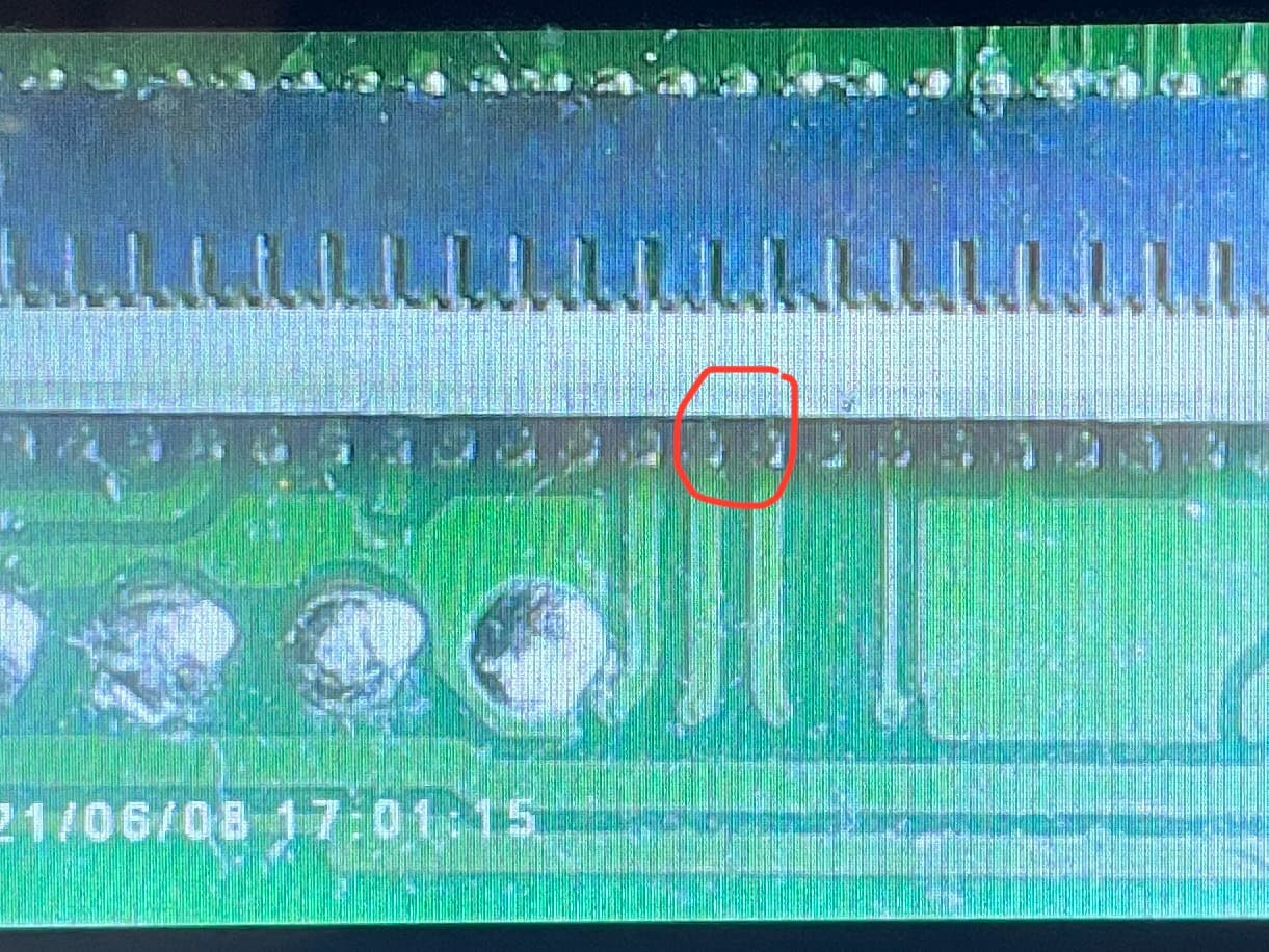
Oh. My. Goodness. How did you know?! Look at that:
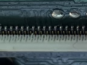
One pin is bent!
It’s actually left a mark on the ribbon cable (or is it the opposite? the fold caused the pin to bend?)
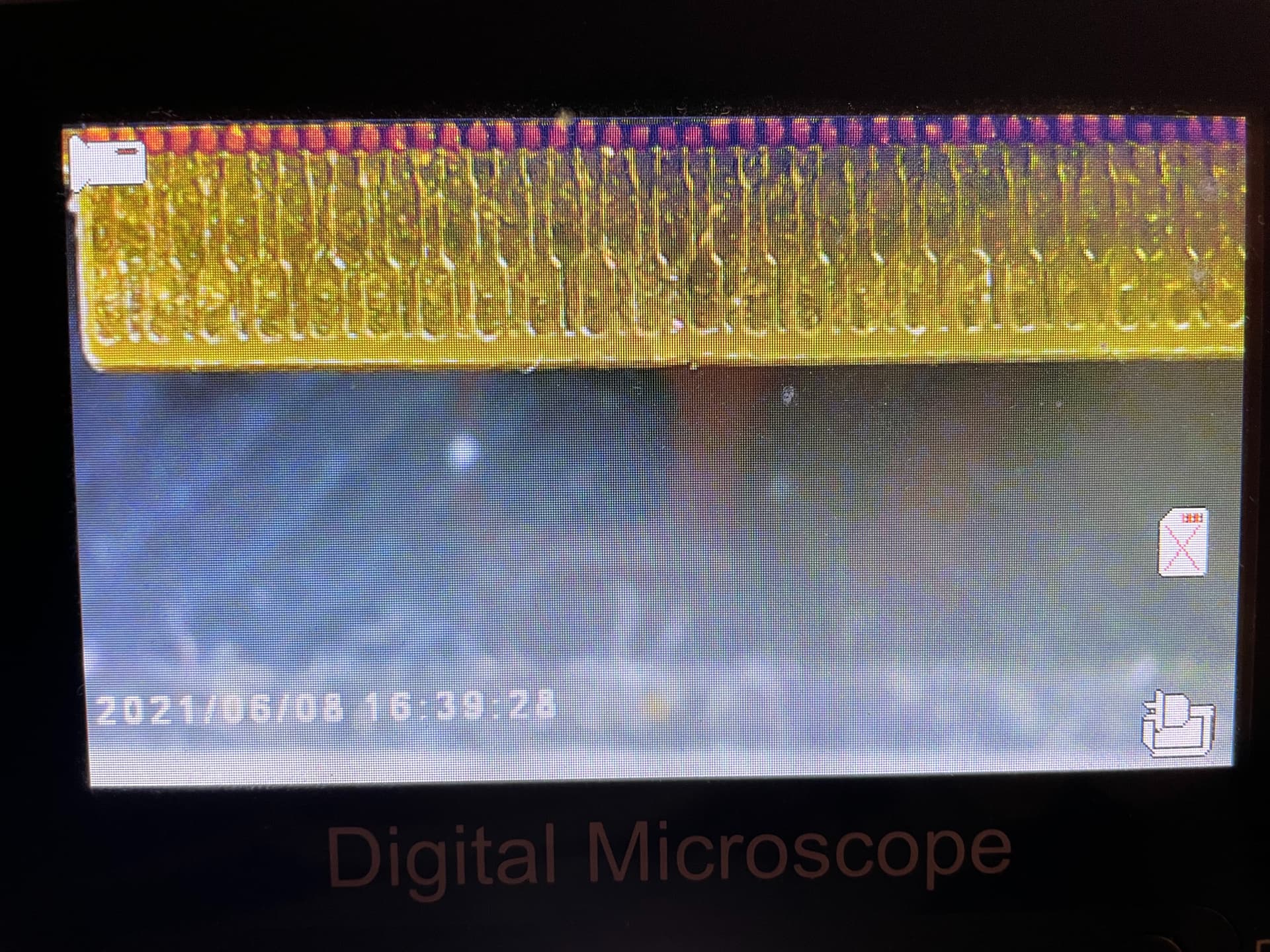
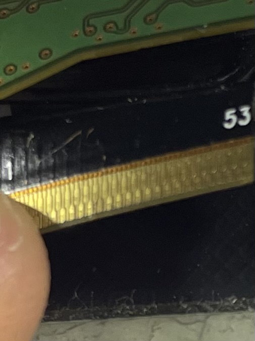
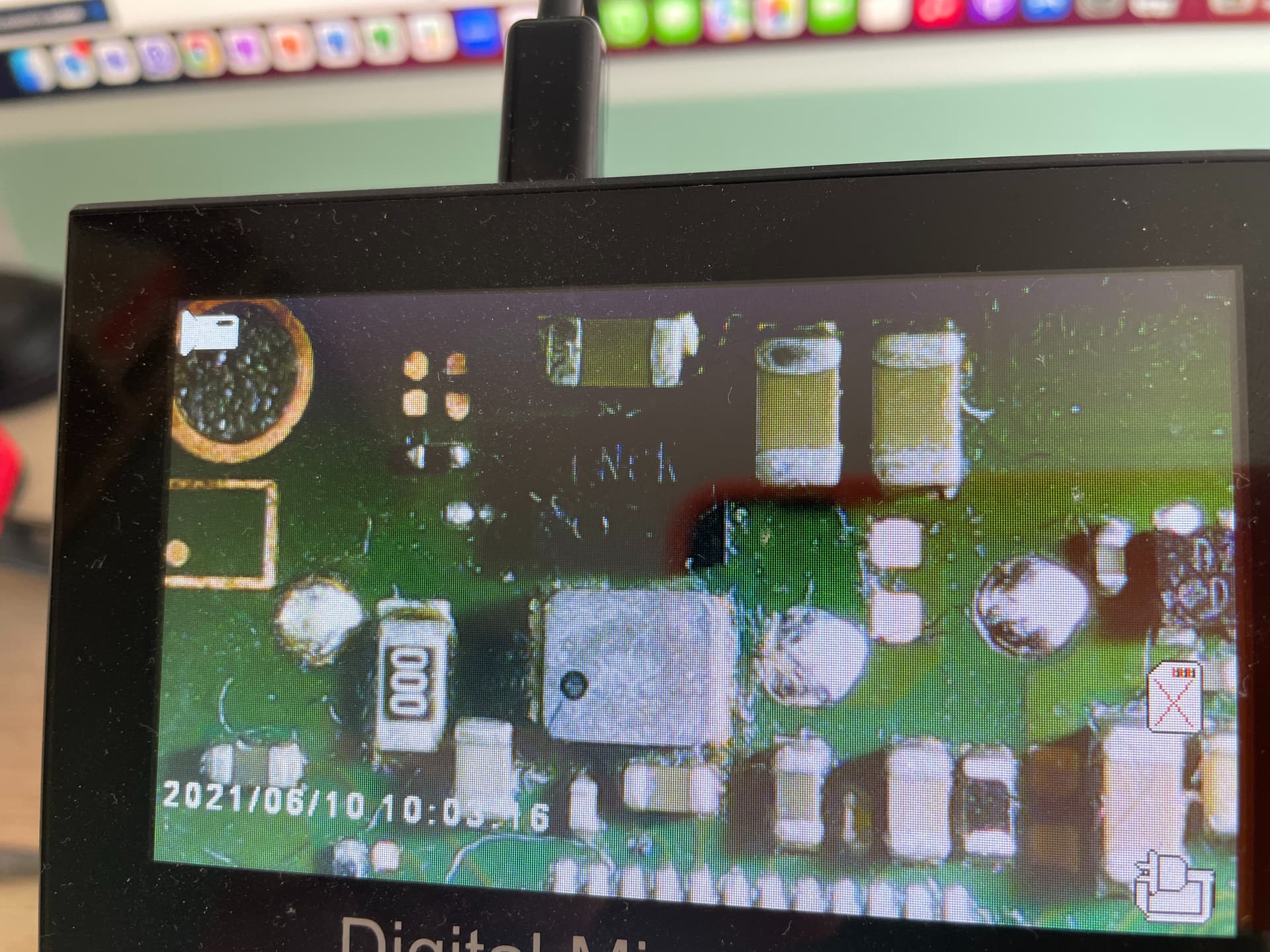
It may not be easy to tell on the pictures, but it’s very obvious on my crappy microscope!
As a result, the resistance between these two pins is… 0.2 Ohm!
So I think we (by which I mean “you”) found the culprit!
So I guess the next step would be either to bend it back in place, or to swap the connector.
- Bending it back: looks easier, but it’s so thin I’m not sure what tool to use. And I don’t want to break the lever.
- Swapping the connector: I changed a plastic connector once on my laptop, but it was much easier (fewer pins), and there were no components below so I could easily heat it from below. Makes me a bit nervous in this case.
As a side note: I’m so glad it’s not my soldering job, haha.
Haha, psychic ![]() Glad you found it
Glad you found it
That’s fine
This is just typical unfortunately as the connector is terribly designed and it’s all to easy to catch a pin while sliding the ribbon in, on the plus side you probably won’t do it again ![]() The ribbon is likely fine, just give it a gentle squeeze with some tweezers across the contacts to straighten it out a touch before next time, if you feel any resistance while inserting into the connector just pull it out and try again. If you still have trouble IPA can act as a temporary lubricant.
The ribbon is likely fine, just give it a gentle squeeze with some tweezers across the contacts to straighten it out a touch before next time, if you feel any resistance while inserting into the connector just pull it out and try again. If you still have trouble IPA can act as a temporary lubricant.
The pins are quite brittle so you’ve basically got one good bend left in it before it breaks completely.
Fine dental picks work and maybe a sewing needle or pin - though tbh these days I find it quicker to just be done with it and swap it out as you can sink a lot of time into lining these pins back up - but like the Max IC we talked about earlier it depends on experience and how comfortable you are doing the work which dictates the course you’ll take.
You can use hot air from below with this connector too. As long as you don’t knock the board or use insane air, surface tension will keep the underside components in place.
Haha, yeah, seems like your M92 install was likely good all along
1 Like
I’ve just tried bending it back with a sewing needle. Definitely not perfect and wouldn’t trust a ribbon to be taken in and out too much, but at least it’s not touching the other pins… and guess what? 1v8 rail isn’t shorting anymore!
Tomorrow, I’m going to carefully try to insert the ribbon and see if it boots. Then I’ll resolder the M92 chip ![]()
We’re getting there!
1 Like
I’ve managed to put the pin back so that inserting the ribbon isn’t causing any short. Sadly, it’s not booting.
I know it’s stupid because it’s unrelated, but I soldered back M92 (and had to chase the resistor and the small cap again, although my hot air station was at minimum airflow, maybe the temp is too high?).
I get a 0.25 current draw, but something is wrong somewhere. I checked the voltages around max77620, and everything from stage 1 boot is there BUT 3V3 is reading only 1,5V.
I think I read from one of your posts @Severence that it’s connected to pin 6 on M92, which seems to be fine.
I guess I should remove M92 and try to find what’s wrong in the first place.
Sounds like a short on the 3v3 rail and with 0.25a draw you can probably feel the heat coming from the culprit, there are a good amount of components on the 3v3 rail, any physical damage on the ENXX ic?, located above the audio ic
1 Like
I doesn’t “look” like there is.
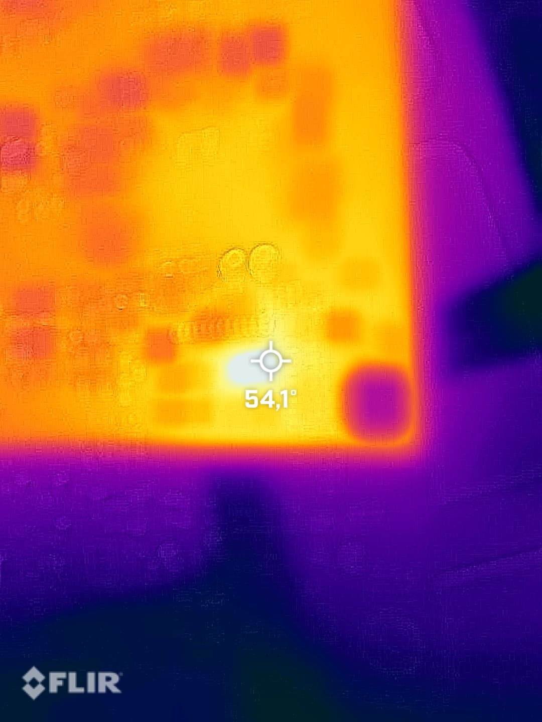
However, I felt things getting hot all over the board, so I took my Flir One out (it’s terrible because of the parallax, don’t get one).
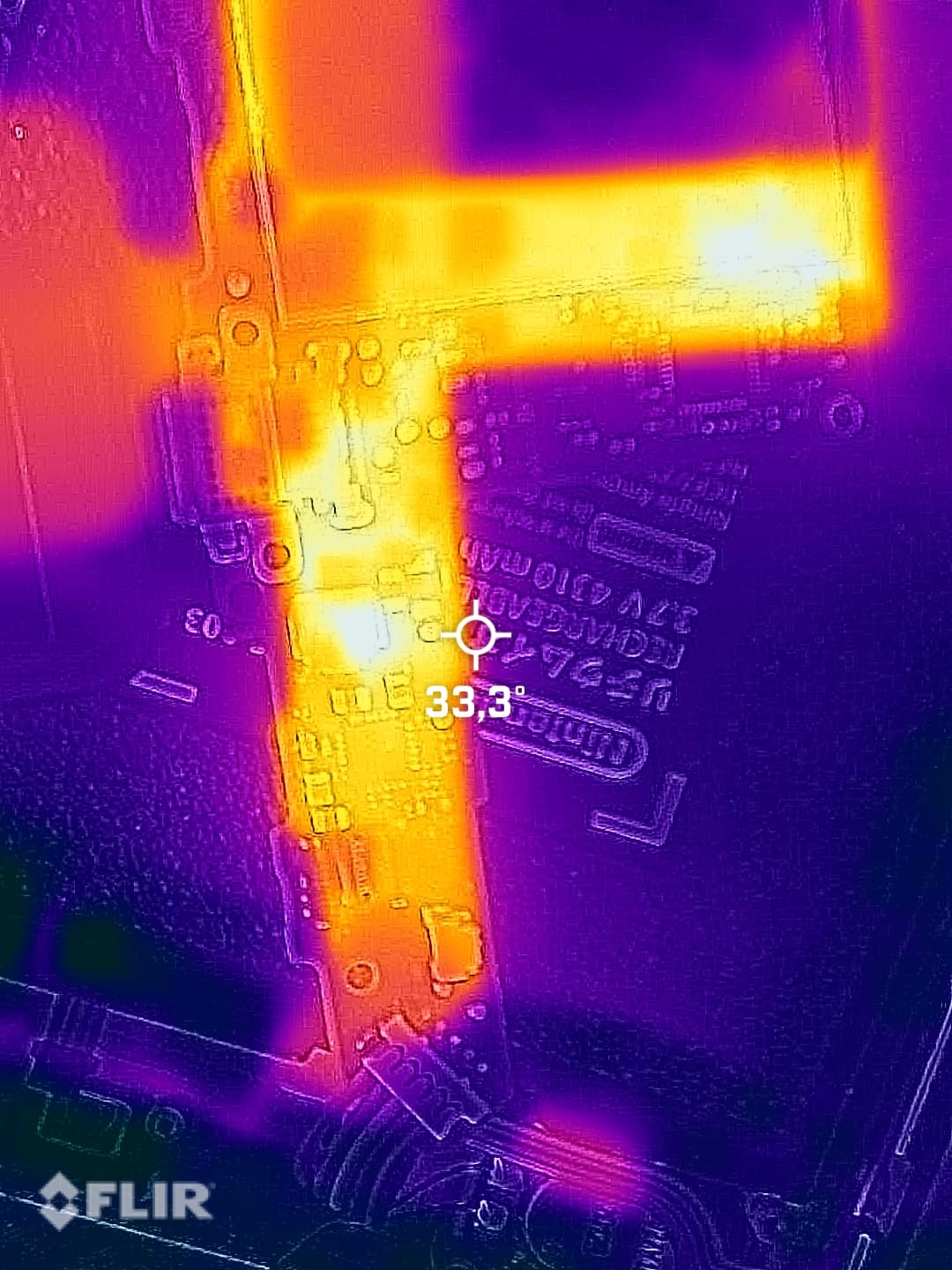
That’s the EN chip.
That’s BQ and M92
I should probably remove M92, and try again, right?
What’s the station? if it’s at it’s minimum and the components are blowing off then best I can guess is your holding the nozzle too close to the board maybe ![]() or there wasn’t enough solder on the pads from the last time and surface tension ain’t doing it’s job
or there wasn’t enough solder on the pads from the last time and surface tension ain’t doing it’s job
Would suggest it’s being pulled down, I’d measure the resistance to ground on this rail (try to get into the habit of doing this so you can identify problems on boards in the future by giving yourself a mental model)
If that’s celcius then 54C is a little too toasty. What I’d do is check a couple of areas around the board as it might just be getting warm as the EN IC is the source/producer. So I’d measure resistance to ground at a few locations where this rail shows up to get an idea, first at pin6 of M92, note the reading, then at the biggest cap near the P13 (this is the most likely candidate as it’s entirely possible that the prior USB issues have taken out this IC) note the reading, then at either of those two larger caps near the ENXX IC - If for example the lowest reading comes up at the M92 then you can safely say that’s the reason and pull the IC, or if it’s the P13 then it’d be that etc.
1 Like
Also just to add to this, I can see what is potentially flux residue (and cotton fibers) at the ENXX IC (though hard to tell from the picture) area and possibly a skewed cap and cold solder on the TP so it’s entirely possible somebody has messed around here and perhaps this problem has only now just reared it’s ugly head or the problem was there all along and maybe just worsened - I don’t imagine 1.5V on the 3V3PDR is high enough for the board to properly function (but stranger things have happened) so I might also take the oppurtunity to check that the 1V8PDR pin at the LCD connector is truly making contact with the ribbon by checking continuity from the rear of the connector to the corresponding “pad” on the LCD ribbon (if you can touch/reach it with your probe) just on the off chance that the console is actually booting (despite the 3V3PDR fault) and we’re potentially dealing with a display issue still
That all being said, I wouldn’t plug in the battery or USB until we have identified the 3V3 issue - we really don’t want to put the EMMC in harms way
1 Like