Okay…
In that case I am getting
V-Out-1 = -5.45v
V-Out-2 = +5.43v
I’m trying to work out which Pin I need to measure on the Backlight…
I might have another question… (this could just be a silly one though)
The Connector next door to the Backlight doesn’t provide power to the backlight connector does it…
because I have not been connecting this one - assuming it is only to control the Left JoyCon
Just measure them all, there’s only three (one out of the four is unused afair, and another is of course ground… so really, there’s only two of interest)
Make sure to measure this directly after injecting the payload - as I foget if Hekate or biskeydump puts the BL to sleep after a while or not
you’ll often freeze tegraRCMGUI when you attempt to inject the payload twice (after you’ve already injected a payload prior without power cycling the console) so imagine this is normal.
Just use the Biskeydump payload here instead anyway, as if you haven’t got the correct files on the SD, you stand the chance of the newer hekate versions not enabling backlight (as, if I remember right, the newer Hekate versions won’t even enable text only mode - unlike the older versions)
~4V is the backlights idle voltage, it won’t actually illuminate until it’s boosted… I think somewhere in the region of > 15V if I remember right, so in other words, you weren’t getting BL voltage at this point.
Your gonna have to break it down and figure out why your not getting USB detection or intemittent USB connectivity before moving forward, either a dodgy cable, dodgy port, dodgy M92 install, or a slip while measuring the BL connector which has now caused a subesequent fault on your SYS rail (I’m just gussing) as an example… if all that checks out, then we are back at square one once again with the SoC being the primary suspect
If you do manage to resolve USB connectivity (some signs of life), Shine a torch on the screen following injecting the biskeydump payload and see if you can make out any of the text or the frowny face you’ll likely see
I might install that new M92 incase it’s the M92 playing up and causing the fault.
I’m sure you said about the M92 being dodgy before… and I was trying to put that aside until the screen was functioning…but it looks like I have got some replacing to do.
How once this is all working do I charge my friend…
How would you charge someone? I’ve put so many hours into this thing and also had to buy many parts, and no guarantee that I will ever come across a Switch like this again….or least hope I don’t for a long while haha
I’d first check the existing port with a breakout board first, then check USB functionality with the cable in both orientations (and of course check with another cable entirely) - Checking you SYS rail too (resistance to ground) only after all this should you consider swapping the M92 IC or port.
You’d charge them for the parts alone, if you get it working you tack on what it would have cost from someone with experience to resolve the problem - IE: the time… and this could be as little as 30 mins (for example)
The customer should never pay (friend or not) for yours/his/her/whoevers inexperience, as we should never be practicing/learning on the customers device in the first place
I’ve got a usb-c test board being delivered tomorrow…
It has a USB-C male plug with breakout connections.
Never used one of those before…
Any pointers on what I’m looking for….
Obviously with that attached I won’t be able to inject payload.
Re - charging someone:
You have a very good point and well noted… I wouldn’t normally practice on customers property…
just on this occasion was trying to help a friend in need and don’t have a practice Switch board to practice on
You just want to check for continuity (using one of the many diagrams online) from the breakout to their desitinations, primarily the ones going to the M92 etc but you can also check the one’s leading to to the P13 also if you want… or just check them all you can also check between contacts (on the breakout) to ensure none are bridged/shorted to one another.
@Severence@zyrex
Hi apologies for the delay in my response…School holidays always seem to be quite busy when trying to keep our sibling occupied.
Re Switch - and latest steps taken
I tested continuity on USB connector with breakout board and everything seems fine.
Although I have not found any diagrams online that link USB to M92.
Checked P13 and all its filters and they are all good.
Reflowed LCD connector and all those connections are 99% better than previous
I have however swapped out the M92 with a new one… but got as far as that so far, I realise than some of the M92 connections need a little bit of TLC with fine solder tip to ensure they are looking shiny… this is my next stage before I connect it all up and test again.
@zyrex@Severence@Insomniac
Hellllpppp !!!
So I now have another problem.
Reflowing the M92 I caused a solder bubble from the solder that was squeezed out from the excess under M92 large ground pad.
Once I sorted the bubble noticed that it took a capacitor that I can no longer locate.
I have searched everywhere and this one is no longer present.
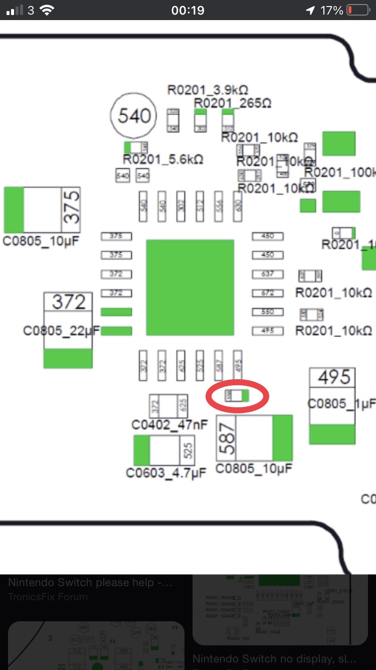
I do not have a donor board that I pull from to replace and have no idea what it’s value is. (See image attached and circled in red
@jkyoho
Many thanks for that information. I will see if I can find one of the same value from a Non switch board.
Might take me a little time now to locate one.
Will be in touch again soon
Solder would not magically bubble out the sides during reflow it happened becaused you overloaded the pads (specifically the central GND pad) and squeezed it down during reflow (bad, bad practice)
check the topic here where I detail why you shouldn’t be squeezing down IC’s
I’ve been seeing a fair number of boards recently which have had rework at the P13, M92, BQ areas by people who utilize this dumb squeeze down technique (evident by tweezer dints in chips and notable board warp in some cases) and in a lot of these cases I also find internal board VIA damage which goes hand in hand with it - these make the boards ultimately unreapairable
I think the biggest issue is you messing with IC’s which aren’t related to your problem, and in this case it’s hard to know if your just creating more problems hopefully once you’ve replaced the M92 we will see a change but tbh I think you should give your customer 20 quid and use this board as a donor and just buy a replacement board for him
@Severence@zyrex
I am currently out of the office at the moment but I have noted the method of how NOT to do it.
Problem is sooo many people show different ways, it’s hard to know what’s right and what’s wrong.
Your advice though and guidance is super helpful…
Only trouble with this forum is when you try and search for something it doesn’t take you to exactly what you need so end up spending hours reading through threads
Yeah it’s pretty tough to know sometimes and often you’ll only know in hindsight. A lot of people use the squeeze down “technique” as it’s a substitute for any real skill (and properly prepping the pads etc) and while it might work in a lot of cases it can cause more problems later down the road.
One way to determine if the vids your watching are spreading bad info is to look at some obvious pointers, for example, if the guy is using a steel brush to “clean” boards (as in what I’d use to remove rust from steel) and scratching the board and inadvertantly trimming resistors… then you can safely assume the guy doesn’t know what he’s doing. If you see a video where he points his tweezers to an IC, inadvertantly grazes and kills the IC and likely the whole customers board and then doesn’t even aknowledge it’s his fault, you can assume the guy doesn’t know what he’s doing. If you see vids where the guy is using a rotary tool (IE like a dremel) on a board to remove solder mask, ulltimately showering the board in copper dust and thinning the copper gauge out, then you can safely say the guy doesn’t have a clue. If you ever hear the term “We don’t have to worry about restoring that pin/pad because it’s just a ground” you can safely assume that guy is an idiot… list goes on, but they’re your clues
You’ll learn a heap from sifting through the different topics on the plus side
@Severence@zyrex
I forgot to mention… I have got a UNI-T UT61 series multimeter on its way to me.
I am going to start from scratch with ALL my readings - yes I know this may seem like a massive task but at least with a proper multimeter in hand I will be able to provide more accurate readings that you Benny and anyone else for that matter can compare.
Re: YouTube videos to watch and follow…I will just stick with Northridge Fix and theCoder that way I will be following more experienced and legitimate peoples work at least.
I will return back to the office Tuesday onwards but thanks for your continued support
No… reread what I just posted and then re-read the other topic I just linked too… this is your problem As I say, I won’t name any names or put anyone down but…