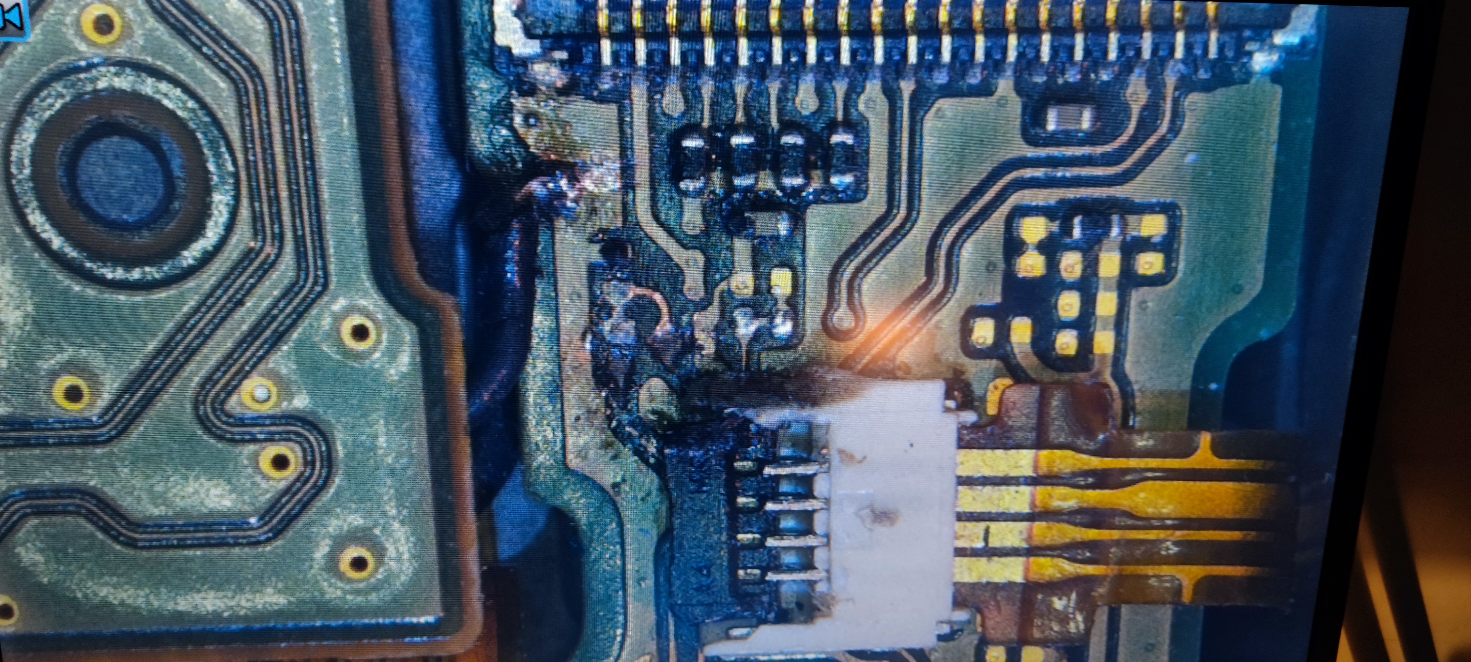
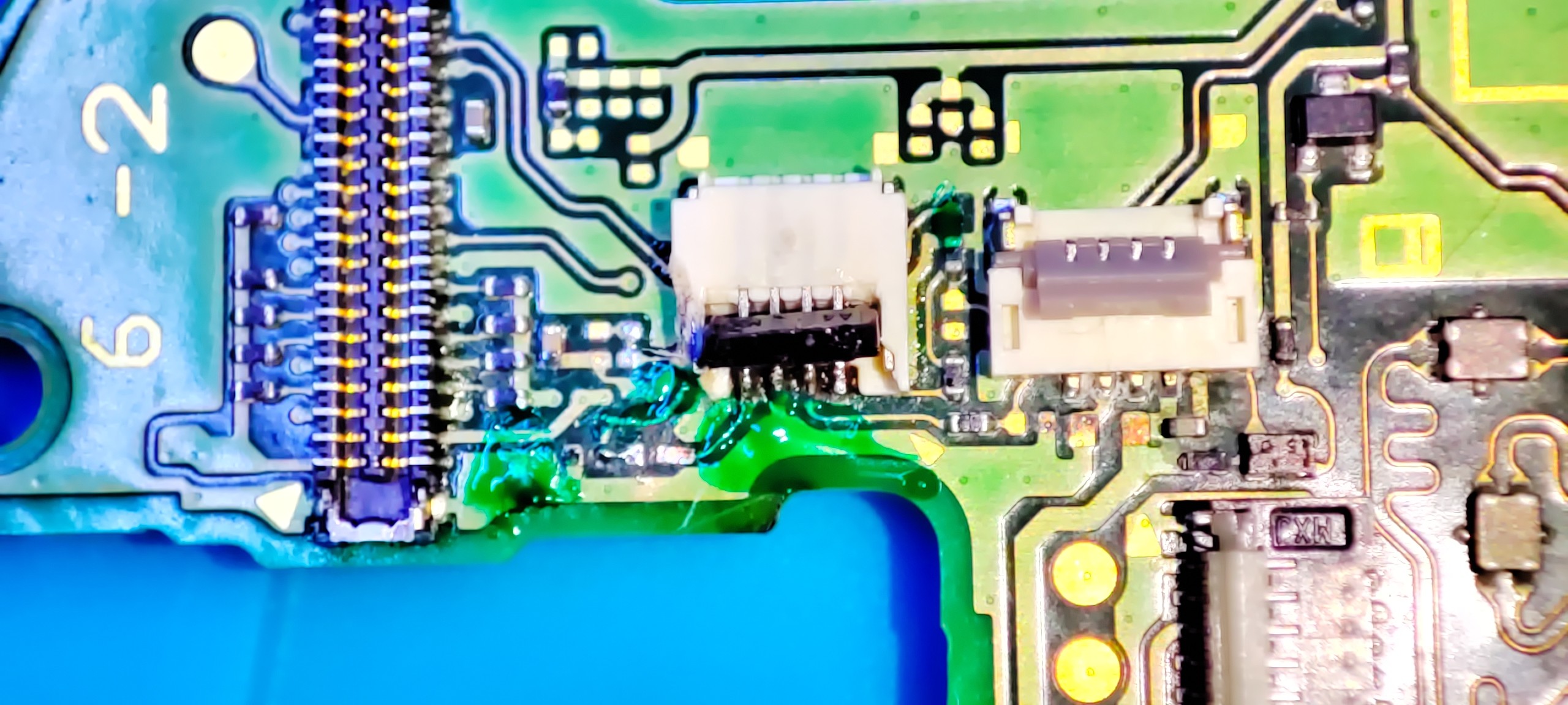
Hi guys, i recently bought another Nintendo Switch that works, charges, both 5 and 15V fast charge, but the power button doesn’t work. I opened the console, and found a huge mess around the power ribbon cable.
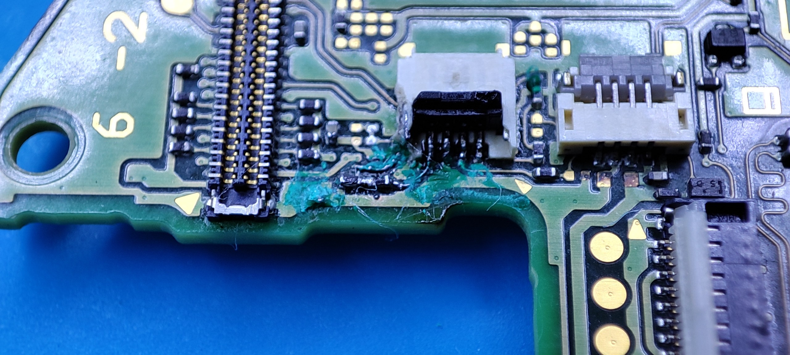
As you can see, the 2 resistors are knocked off, the pads are completely damaged, but what worries me the most is that cable you can see that was solder on the board on a scratched surface and which has a bunch of SMD components soldered to it, and was left like that near the game card reader. Has anyone a clue why someone would do that ???
No idea, I can imagine someone deciding to jump a wire to the gamecard board had a damaged ribbon or something, but there are cleaner ways of fixing it.
Given the rest of that area I would assume they had no idea what they were doing, and remove it, clean it all up and try and fix whatever is broken properly…
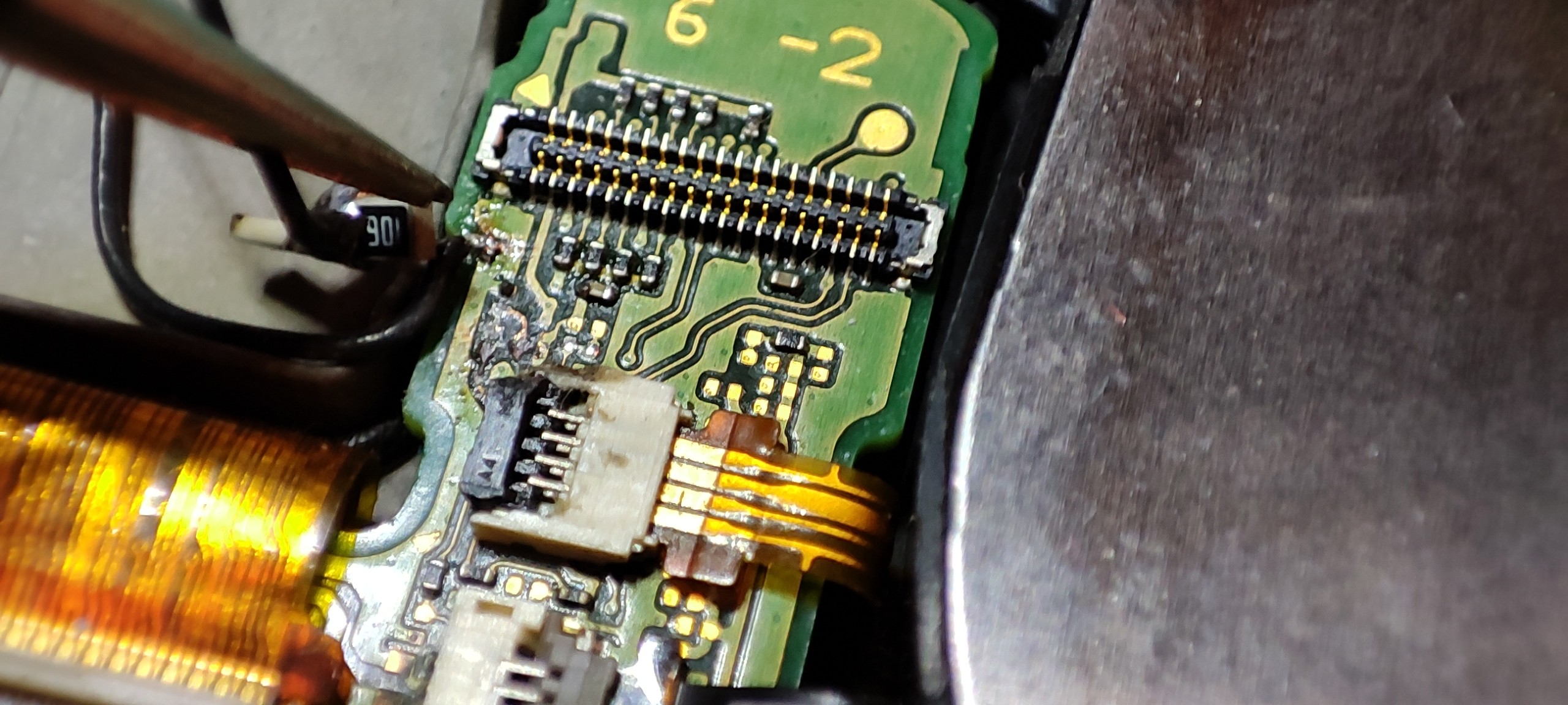
I have fixed this. This was wrong with the one in my other thread. There is a trace leading under that connector you cant see that the two resistors lead to. On mine it happened to be mostly ripped off. Just south of this is a test point of aforementioned trace that I installed a small board with the missing resistors and lead the wire up through the vent directly soldered to power button PCB.
If this trace is still there you may be able to replace those resistors to get it working, but i got frustrated with the size and used larger parts by the test point
I will get pics. Once I worked it out it ended up being pretty easy to fix.
Hi FCE, that would be awesome, thank you in advance for that. I actually saw in one video from i think northridgefix that resistors and pads were missing or it was another one, i don’t recall exactly.
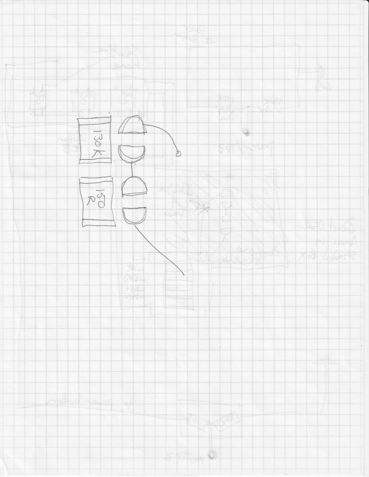
Okay, I’m going to break this into two posts. What should be stock and how I fixed mine. I had more damage than the usual so I had to figure out how to rebuild the part of the circuit with the resistors going to the power button.
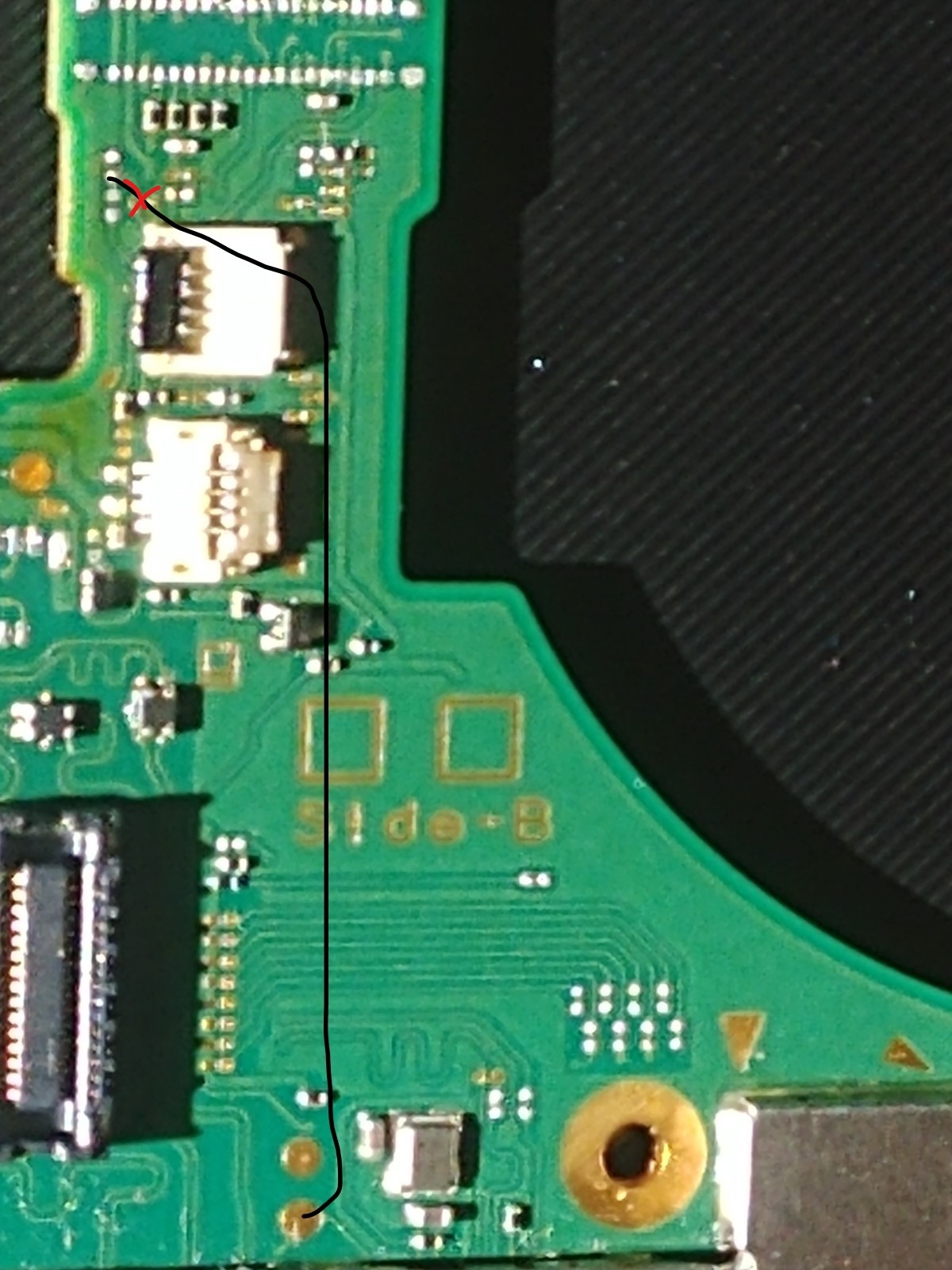
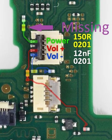
Here is a V1 donor board with the traces marked out. The resistors are already missing in the photo.
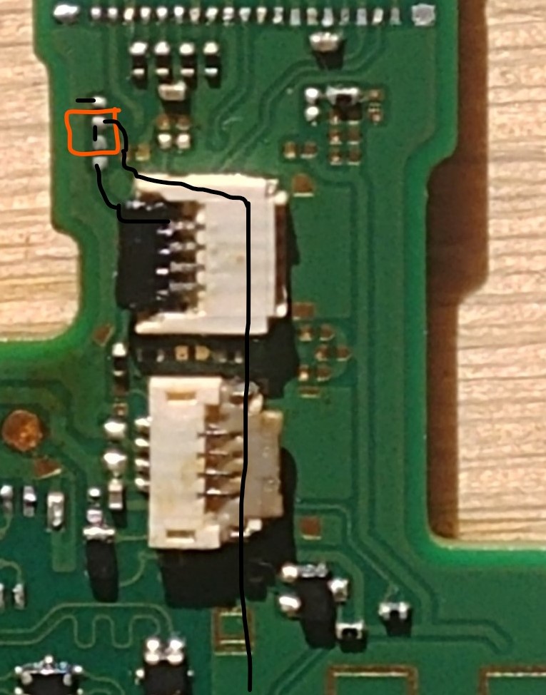
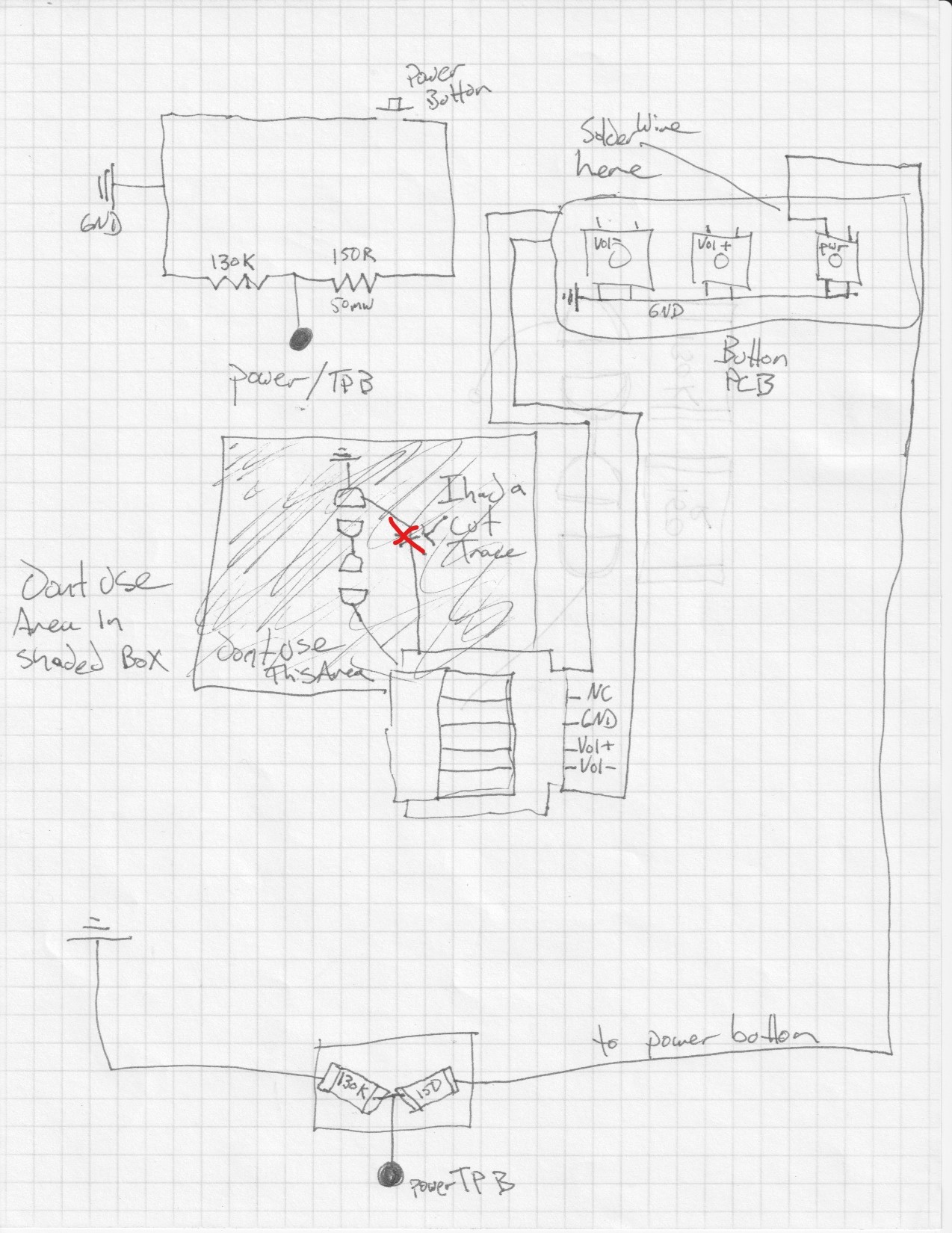
Looks like you have V2/Mariko methinks. Here is drawing of what I see on your PCB. Slightly different layout V2 has VIA, not on V1, but exact same concept.
If the resistor traces are still there and the via to the test point is still good all you have to do is replace those two resistors, but you have to be super careful not to damage the plastic on the power connector if you use hot air.
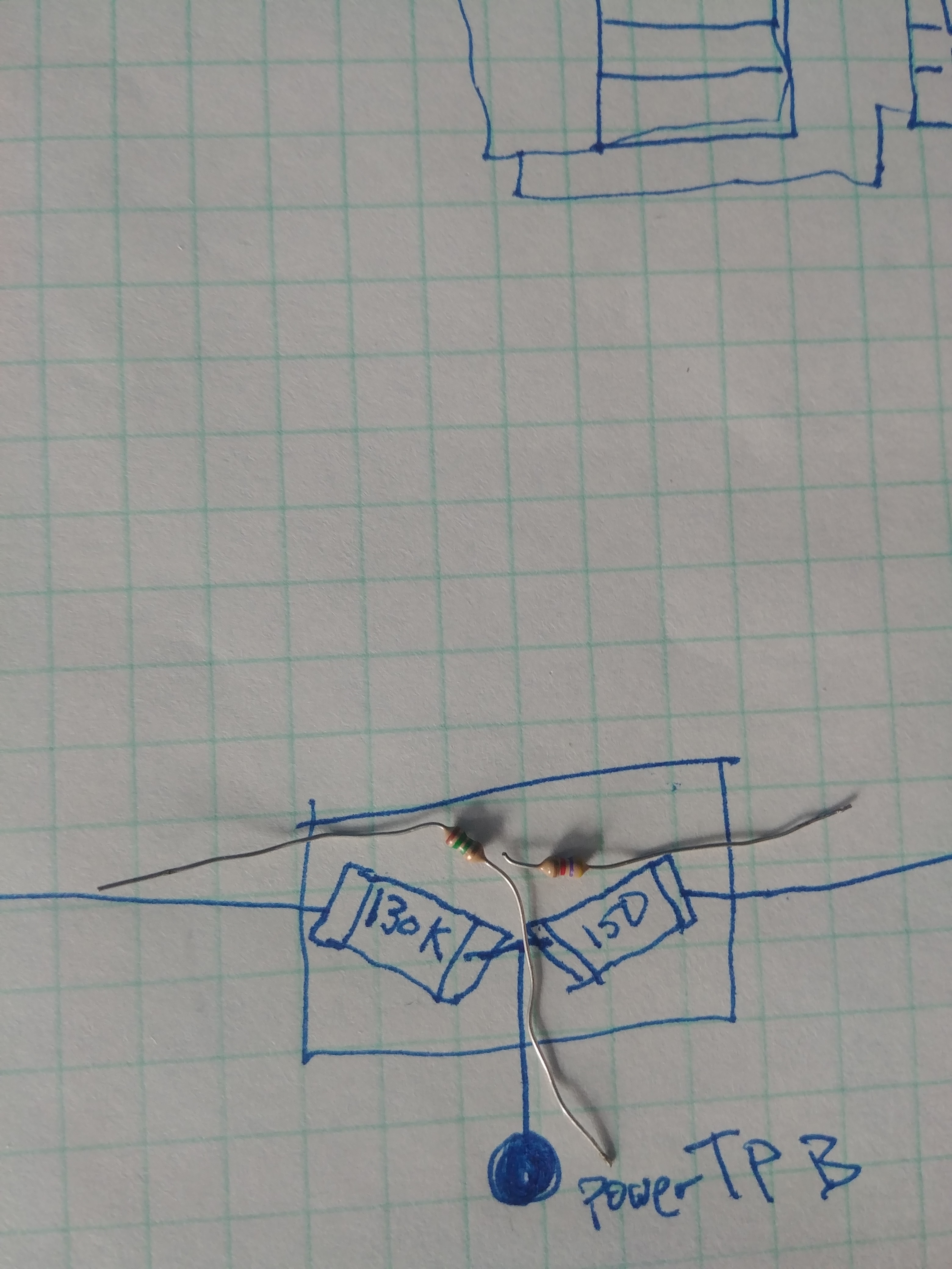
Mine had the trace going under power connector/through via removed from damage. I kept trying to replace proper resistors not realizing I had this third line sprouting from between the resistors. I got so mad knowing I knew I had them on and it wouldn’t respond… I ended up losing the resistors and mucking up traces. At that point I had to take the resistors to another small PCB, lead it to TP, GND and the power button. I will explain in in pics next post.
I can’t for the life of me remember the values but I will track that down.
I found the power test point(what I call “TP B”) on V1 by looking at other folks documentation online. Read it out with multimeter(should be easy not many in the area V1) or find it on V2 PCB with test points marked in photos.
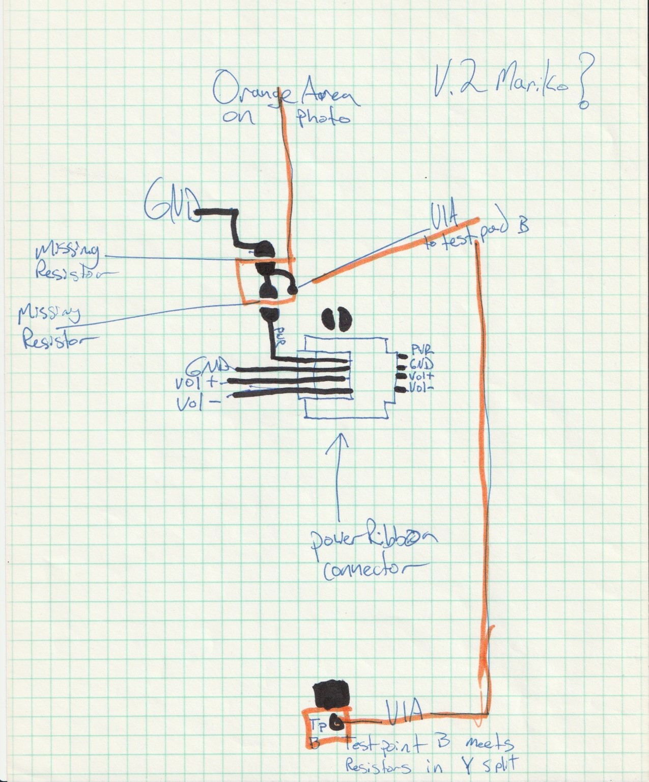
Real quick I feel I need to explain what I call power or “TP B” This is not a voltage line. This is an input or output from a processor to the power button. You must find this trace/test point. Do not put a voltage line on the power button.
So in theory all we have to do is replace the resistors. The one towards top of board going to ground is 130K and the below is 150R.
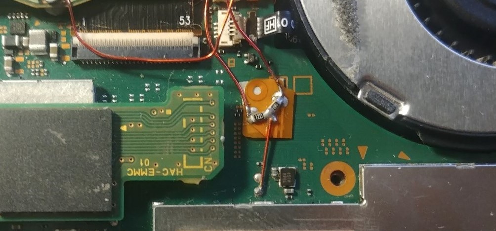
The trace had been removed before I got my hands on it. I decided to use 0605 resistors I had on hand and take it off the main PCB. This way I wont damage the power connector anymore as I’m nowhere near it. I actually use an iron not hot air for 0605 in cases like this anyway.
In the top left is the schematic of what must be accomplished. The power button on the button PCB is directly wired to a daughter board with 0605’s that also connects to PWR/ TP B and ground. I bypassed the section on the board where the resistors used to be. These real life shots dont show everything but its enough to get the idea.
Hi FCE, sorry for the lack of news, but i am really busy at the moment and couldn’t spend any time on those Switch so far.
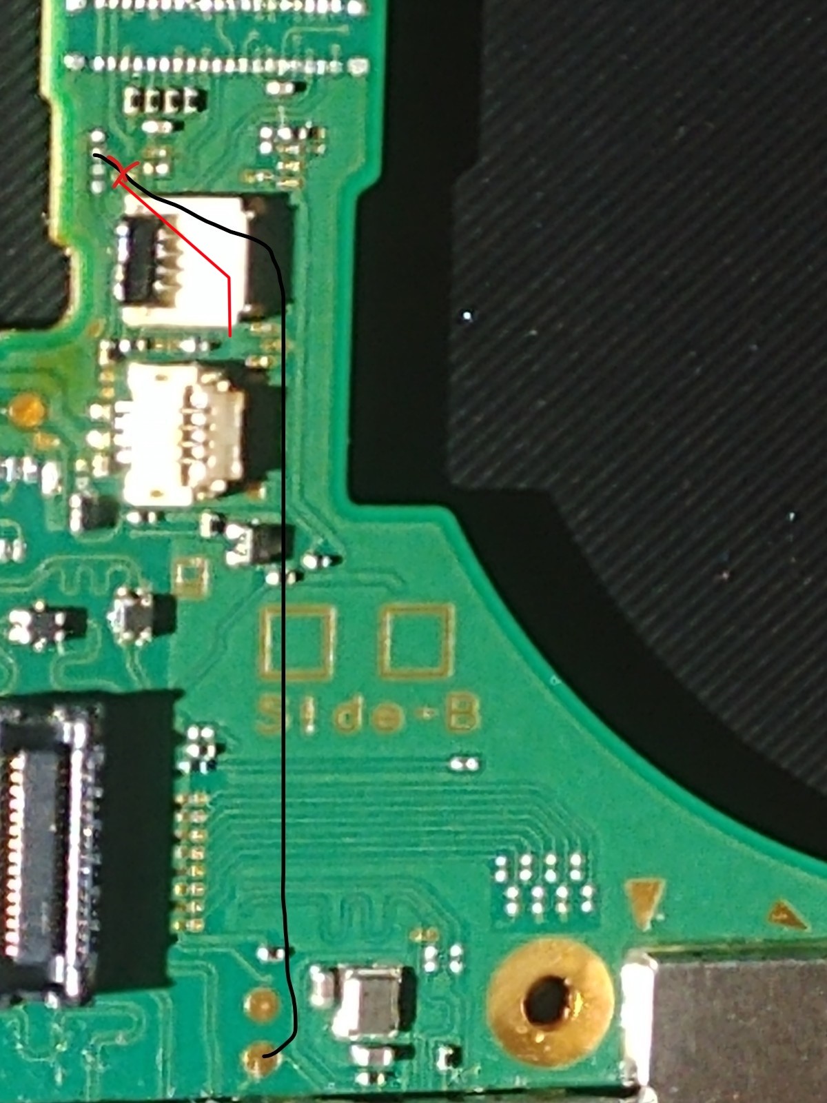
I finally managed to have a look for the one with the power button missing. I repaired all broken traces, solder jumper wires and missing pads and applied solder mask. I know it isn’t a perfect job, but it looks to be ok on continuity level with the multimeter now at least.
I didn’t run down like you showed, first because i still had a small trace available on top left of the connector to reattach the missing test point and trace that goes in between the 2 resistors. And second, i found a shorter point where you can lead your jumper wire, and it is in bottom right of the connector, you just have to scratch because it isn’t a test point but a via, but still it can do the job i guess.
By the way, i checked the wire that was in previously, and i think the guy attempted a repair like yours but didn’t succeeded and leave it there because there was the same smd resistors as on your picture.
One last thing, when i measure the resistance on a good board, i found indeed the 150Ohm for the below one, but the one closer to the ground appears to be a 10M Ohm, is that normal ? I measured 2 different boards to be sure.
Hi everyone, repair done, console fully functional, i placed the same value as you recommended, and i confirm that with 2 resistors it is working perfectly, so i don’t know why on the picture it stands it is a capacitor, FCE is right, 2 resistors are doing the job. Thank you again for the help, problem solved
This why I used 0605s. Great job man. Resistors and or caps can read wrong in circuit due to the traces they are attached to. Ive had Caps read all sorts of goofy in circuit but if you remove it it measures perfectly.
That picture is not at all clear. I think the 12nf is referring to the cap at the bottom of the pic attached to the red line.
Ive been coming across this pic for two years and I think the above finally explains what was trying to be conveyed.