V1 with Blue Screen, takes payload but doesn’t boot Hekate

Hey everyone!
I have this switch from a faulty job lot. It’s displaying a blue panic screen, but unlike others I had it’s not booting when pressing the APU or the RAM.
So instead of just blindly reflowing (poke @Severence ) or reballing, as I got myself some stencils, I thought: why not use your brain for a change?

There was no serial number but I suspected it was a V1. Setting it in RCM worked and injecting payloads too.
I can access a few things, but hekate isn’t booting (something about « Minerva »). Now I’m not sure why a Roman goddess would have anything to do with it, but is it possible that it’s not a hardware issue?


Thanks in advance for your help!

Just to be accurate: the first screenshot is because the sd card reader wasn’t connected. On the second one, it was. On the third, I removed the SD card AFTER getting the error, to bypass it and access information on the Switch.

Hey there.

Try using an older version of Hekate, text only mode (no SD adapter connected) and see if there is a change. All indicators for that error code point to SD related issues so if that’s not the cause then naturally we’d assume SoC issues given the no boot stock / BSOD symptoms. That being said, you may not be able to boot stock for unrelated issues sych as EMMC/fuse mismatch issues (though less likely)

So yeah, try booting a text only version of Hekate, you may also want to disconnect the EMMC module prior to this too incase that has problems and if it boots check out the info pages so we can rule out a potential fuel gauge issue. If Hekate text only still fails to boot then further reinforces SOC related problems in which case might be worth trying Biskeydump payload and seeing if you get artifacting on the display which would further reinforce SoC / Ram problems :+1:

1 Like

Thanks for the procedure.
So I booted “text only”, with and without the EMMC.
Looks like the SD card reader is fine, and the fuel gauge too.


Biskeydump provides some interesting things.

  1. The little smiley face is moving, there’s colour, no artifacts, so I have feeling it’s not completely braindead
  2. That error TSEC FW CRC32 INCORRECT… that sounds like an error with the firmware… Could it be the EMMC/Fuses mismatch you were referring to?

I don’t think your EMMC is a match for that board I’m afraid unless maybe it’s because of Biskeydumps age.

You can give lockpckRCM a try if you want and/or use Hekate (I think you can do it in Hekate text mode too) and see if you can get your BIS keys or get an error etc (sorry I don’t remember the names of the pages/buttons/names etc you need off the tp of my head, been a while)

I suppose it’s possible the data is corrupt on the EMMC :thinking: bit hard to tell at the minute, I’ve seen some boards boot with a BSOD with the wrong EMMC connected and some not, just the black screen as you’d expect. Seems to be dependent on what stage / partition it makes it to / starts executes

  • I tried a different reader just in case, but no dice. Whenever there’s an SD Card, it prevents Hekate from launching.
  • Lockpick hangs when trying to dump the sysnand.
  • Hekate (text based) does something strange when trying to read the eMMC info. It starts displaying things and immediately drops then hangs.
  • I tried a different eMMC (but I don’t think it’s a v1, don’t know if that matters). Same behaviour, but it’s displaying more things. I used the slow mo feature of my phone to get an image before it drops

So it seems to go further into the eMMC. Again, it’s not the same revision as the original one.

Maybe there are other payloads that could help me retrieve the keys. If I can have them, then I suppose I can rebuild the NAND…

Givien the issues surrounding the BSOD and then also the SD, and EMMC issues all of which go off to the SoC, that is where the finger is seeming to point. I suppose it’s also entirely possible you have two issues, wrong EMMC to SoC pair too, though I guess less likely.

You’ve gotta be a bit careful with this as you can inadvertantly blow update fuses duing this, not a huge deal in your case as the patient is unpatched (so you can get out of a black screen stock boot scenario) but it may cause you confusion later on down the road during dianoses and muddy the water.

If the SoC is bad or has open lines to/from the EMMC then it makes sense it can’t get the keys which aligns with what your seeing in the tools afaict, could also be the data is corrupt on the EMMC on top of that too.

So my best guess atm is SoC issues and most likely SoC / mainboard joint issues, while you can reflow I started leaning more straight towards a straight up reball of the bat as if the reflow fails you wind up exposing the SoC to multiple bouts of heat and it’s quite heat intolerant. Also Switch SoC is a bit of a challenge if it’s your first time to reflow or reball, you’ll wanna manually preheat the reverse side of the board prior for a good amount of time with your hot air gun (assuming you haven’t got a preheater) and after, during reflow or removal of the SoC keep a keen eye on the resin around the central die, typically when I get them in and techs have done work like this, the resin has turned brown or black which is basically a death nail :frowning:

I’m afraid so. It is as if the SoC was starting to read the eMMC but then would fail mid process. I don’t really know whether that made sense or not, but I also checked my eMMC connector for open lines (without the eMMC plugged in). Unfortunately, everything looks “normal”. I’ve been searching all over that forum and GBATemp, but I don’t see other suspects than the APU.

I still haven’t made up my mind: reflow or reball. I have a spare donor board with an APU I know is good. Maybe I should practice on it first.

Anyway, what I find frustrating is that that console is still giving me something, since I can inject payloads, access them, display things on screen without artifacts… I also find the ineffectiveness of “pressing the SoC hard” slightly disturbing: based on my experience with BSOD switches (which is like, 2…), it would allow for the console to boot…but not here.

Switch’s which don’t boot into the full Hekate gui or give BSOD is a pretty common occurence on consoles which have SoC / joint related issues. In other similar cases, Switch’s which show artifacting are typically a similar problem but usually issues relating specifically to lines going to Ram which is why often times the symptoms can be “relieved” by gently pressing on the SoC or Ram modules.

While a reflow is a perfectly valid method (provided no liquid damage or board warp or hard joint issues ie: damage pads torn usually as a result of board warp), I do try and avoid it these days if i can to validate those other potential issues prior. IC datasheets used to specify the number of times said IC could actually be reflowed and the times and temps, now it’s just assumed that the IC will only be soldered once given that we are not in a repair culture anymore, they used to do this because any amount of heat above the “safe operating temperatures” and again “maximimum operating temperatures” as laid out in the IC datasheet can (and in all liklihood will) degrade the IC in some form or fashion, I wouldn’t be surprised if some guy benchmarked a GPU and if I was to reball the main wafer, even perfectly, even with a 20k rework station and dedicated profiles etc etc that afterwards the benchmarks would likely show a notable difference/degredation in real world performance, I only mention all this so people are aware :slight_smile: Switch SoC is a sensitive little flower to begin with :wink: as is the board itself. practice on an SoC which you don’t care about if you’ve got one as oppsed to a working one (uness of course that other on doesn’t have a matching EMMC module for it) :+1:

I finally opted for a reflow, with probably the wrong assumption that it was probably just a minor faulty thing causing the blue screen.
The reflow itself went pretty well, nothing fried and the resin around the dye remained grey. I’m also 100% sure the solder melted.

Anyway, I gave it a test, and still the same blue screen. After injecting a few payloads however and mounting/unmounting my SD card, I think I ended up killing it (the SD card). When plugged in my computer, it’s recognized but impossible to format…

So maybe it’s not the SoC. Or rather: maybe it’s not how the SoC is soldered to the board, but rather the SoC itself (internally) or something else completely. The fact it starts reading the eMMC partitions then drops is puzzling me.
Also, since it’s a v1, shouldn’t I be able to boot hekate even without an eMMC ?

If your still failing to dump the EMMC (incl your other module you tried earlier to rule out an EMMC fault in and of itself) following SoC reflow then it still implies SoC related issues

Yeah Hekate will ordinarily bbot (with GUI) without the EMMC connected, but it’s typical it won’t boot into GUI when there is SoC / Ram related issues.

In regards to your SD card, try using HP SD formatter or rmprep USB to format the card instead, sometimes when corruption occurs, windows will just flat out refuse to do it properly… typical windows

Sure, it makes sense. The inability to boot the GUI points to that direction too. Is it possible the SoC itself is partially bad?

Not sure what to do next:

  • Re-reflow? Not sure it’s a good idea, considering what you’ve said about how many times a chip can endure such heat
  • Graft another SoC from a donnor board? That would require me to remove the working one, reball it, remove the faulty one, solder the new one in place. I’ve never done it. I guess it’s a great way to learn, but it’s a project in itself.
  • Consider that one gone and move on. Which sound like quitting :wink:

Right, but just to mention to boot to Hekate gui you also need the required Hekate files on SD too, and if SoC has issues with the SD related lines then this too will prevent this.

Yeah, if it didn’t work the first time it’s unlikely to work the second.

This assumes your current patient board is good (I have my doubts) and it also assumes that your donor SoC has it’s matched/paired EMMC module with it.

For sure :+1: but you will require the special jig (bronze coloured one) as most of the alt ones on the market the SoC will not properly fit or be held. Likewise you’ll need the correct stencil for the jig, solder balls etc etc and you’ll prob wanna get Ram stencil while your at it too as they usually go hand in hand.

Solder paste wouldn’t work?

Not really, I mean, I’m not saying it’s impossible with solder paste but it requires quite a bit of experience, the right jig, the right paste, the paste has to be the perfect consistency / in date etc etc . So easier to just say no and that the only option is jig, stencil and solder balls (which tbh gives a far more consistent and better result anyway)

I should be getting all the required material this week. Looking forward to giving it a go.

In your experience, is the fact that hard-pressing on the SoC doesn’t change the behaviour a bad sign or not at all?

Well, you shouldn’t be hard pressing on the SoC tbh as as the die is essentially a thin sheet of glass and doing so could cause internal fractures. gentle pressing is fine.

In regards to what it tells you, not much tbh, could be the SoC itself is just dead.could be board damage (layer delamination etc) causing the issues, could be SoC joint issues or board pad issues, could be ram issues (or corresponding board joint issues) on top of SoC issues. Most of these issues above, no amount of pressing on a chip will resolve.

If it were me, given all the problems Id probably shift the SoC (and EMMC) over to another board, preferably one that you know is good or is relatively good.

I gave it a go this evening.
I have to say: if you’re patient enough and don’t go crazy with the heat gun, removing the APU isn’t that hard.
And with the right jig that doesn’t bend, so is reballing. I went the solder paste way, a pretty smooth experience.

When inspecting the board however, I found this.

Now I can’t be 100% sure, but I don’t think I did this. Could this be the issue from the very beginning, which would explain why a reflow or pressing the chip didn’t do anything?
Is it fixable?

Yeah I think it is…
Had some pads lying around.

Nice Job :+1:

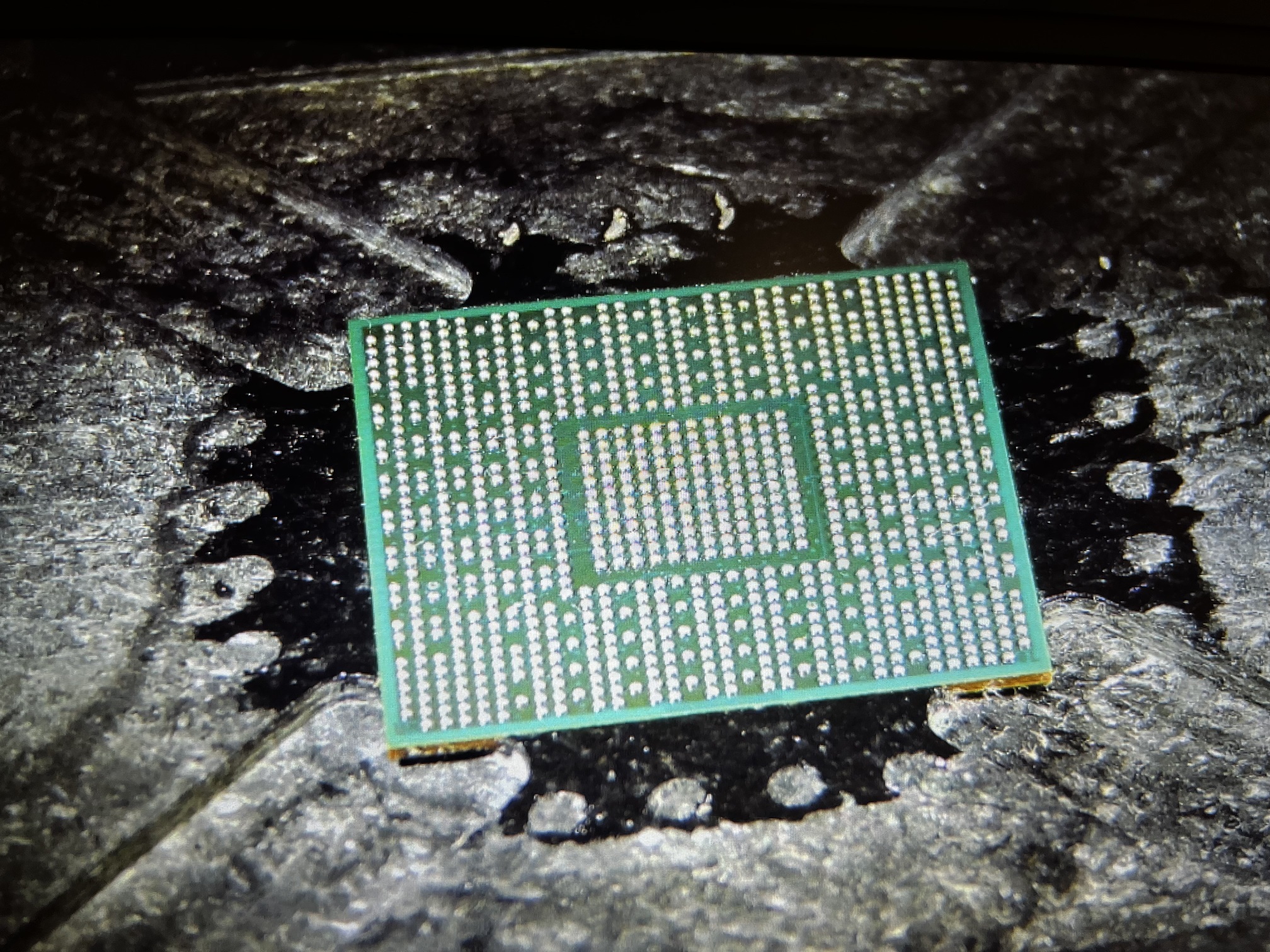
Just check the balls are a consistent height to one another, it’s near impossible for me to tell from your picture. For example, if you have even one ball which, let’s say, is 20% smaller than the rest, then that will likely not take to the board come reflow time, whereas on a smaller IC you’d probably get away with this, simply because the area is smaller. Also just to mention, using stencil and paste on packages of such a large size aren’t nearly as forgiving in general when compared preformed solder balls not least for the reasons I mentioned above but also because solder paste will always result in smaller balls when compared to factory/preformed balls, this is simply due to the flux content in the paste and/order hole size in the stencil… theoretically the stencil manufacturer could compensate for this by altering the hole size in the stencil… but they never do. What I’m getting at here, is, if your board has any amount of warp/bend etc preformed balls will help you out in this instance (I mention all this as it’s connected to what I’m going to say next :wink: )

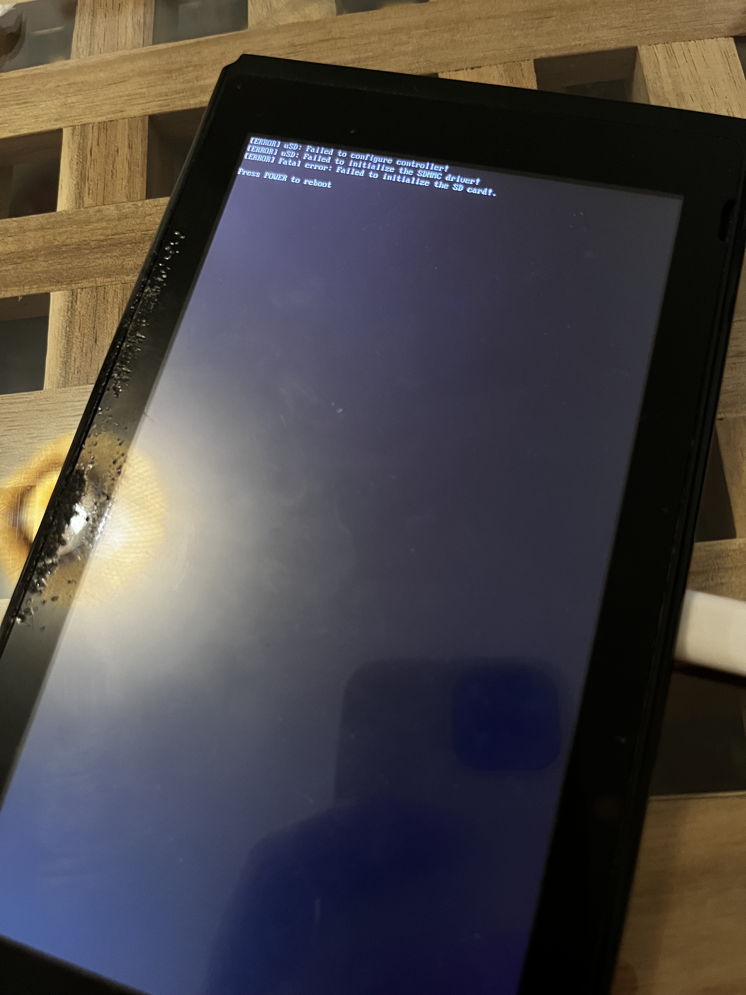
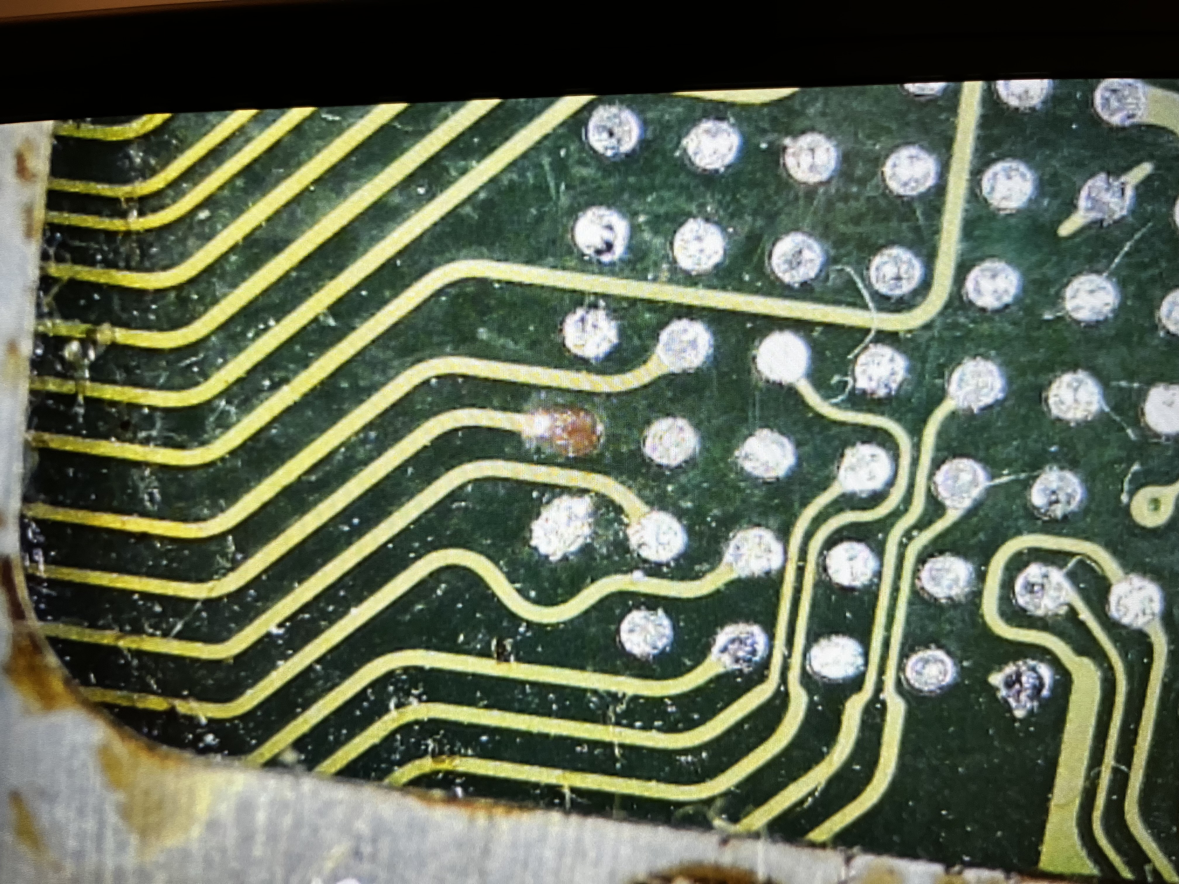
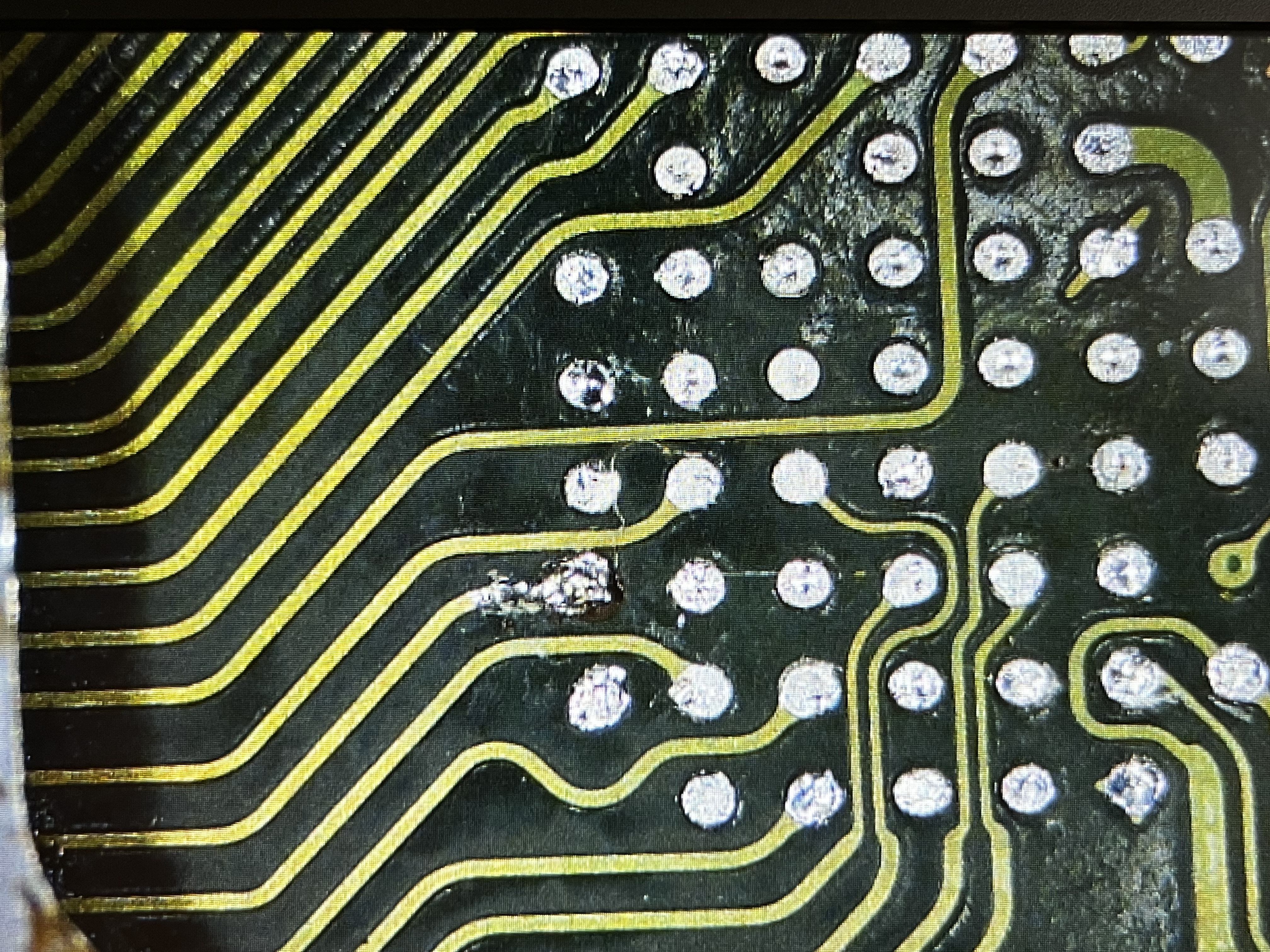
This is a little hard to tell if this was existing or caused by you during removal or wicking, but, those pads/lines going off to ram and this failure mode is typical on boards where the chassis has a bend (however slight) and the worst of the bend typically happens to the left of the USB area, ram and this edge of the SoC. I’ll often see those pads disconnect from the trace or, for the pads and the traces to pop up completely (incl the ones ram side) , I’ve even seen the whole row come up with the SoC during removal… I have repaired them in a few cases, though I tend to avoid it if I can and instead transfer the SoC over to another board. I’ve also noticed this issue on boards where people have replacesd the USB port… and I guess have mirrored the moronic YTer who basically mashes the USB port down come reflow and looks like he puts his whole body weight behind it :upside_down_face: , which basically induces a bend like above, and then the board gets screwed back in to it’s flat chassis and the pads/joints/traces shear off or they fail over time.

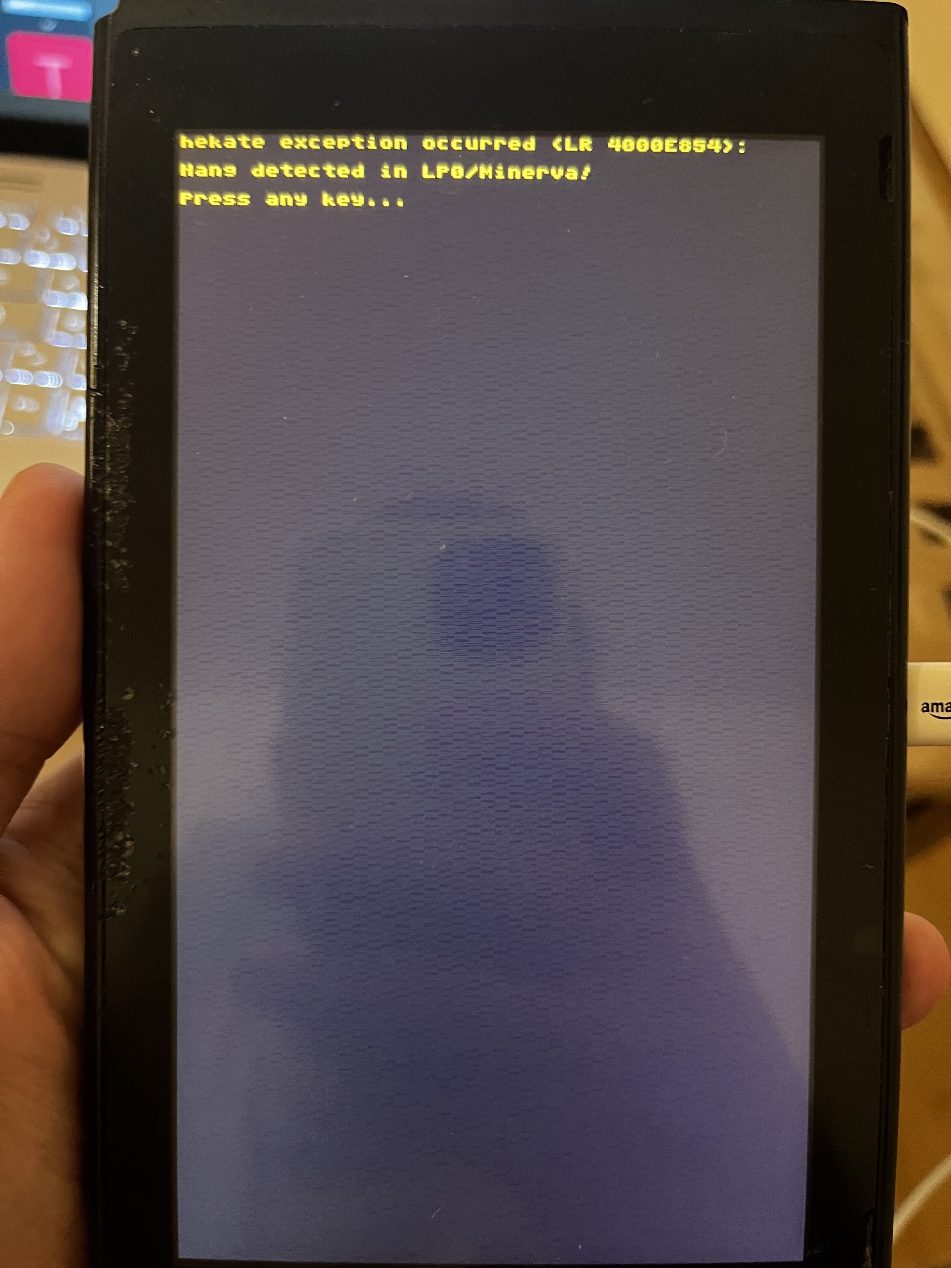
Hard to tell from your image but you’ll want to use UV mask on edge if you haven’t done already to help hold that pad down otherwise it’ll just get sucked up come reflow. You’ll also wanna check the other pads at least on that row too, poke at them and see if any feel spongy, scratch back the mask on the corresponding traces and check continuity etc as sometimes in the cases I mentioned above, there will be a break which is near impossible to see, typically at the pad itself. Depending on the outcome, you may find some of the pads at ram will have the same issue too, so worth keeping that in mind.

Trouble in cases like this is, you may go to all the effort to find and fix the damage, but there may be trace damage on the internal layers too, so even if the repair is successful and everything works great following, problems could still occur later on which is why I do try avoid reusing boards in these cases, particualrly if I’m doing the repair for someone else or intend on selling the device… thought it worth mentioning :slight_smile: