V2 Nintendo Switch has left me SO confused

Hello everyone!

I’m new here, but I really need help with a faulty V2 Nintendo Switch I repaired, but somehow broke again. Let me tell you my tale of woe and… confusion:

(TL;DR: Repaired faulty V2 Switch, then installed HWFLY modchip which worked fine, but Switch needed to do an official firmware update to allow use of a Micro SD card. Update suddenly stopped modchip from working as it kept booting to OFW. Tried reflashing modchip several times, still wouldn’t work.

After opening back up to check soldering, removed modchip and Switch wouldn’t turn on. Replaced some capacitors on APU, but no joy. Can’t see any trace damage and can’t tell if anything is missing. Please help!!!)

So, I grabbed a faulty Switch off eBay which had the description of no power but good cosmetic condition. After assessing it, I saw that the USB C port was knackered. I’ve read a lot of posts and watched a lot of YouTube videos to know that this can cause all sorts of components to die. What’s worse is that someone else was inside this Switch before.

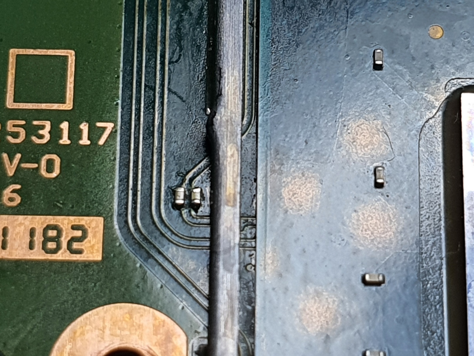
I replaced the following: M92T36, PI3USB30532ZLE, BQ24193 and MAX17050 as well as a few 0201 1uf capacitors. I picked up a donor board for extra parts and for the USB port as aftermarket ones didn’t seem to fit as good as a genuine one (sadly it was a V1 board which the seller pretty much lied about, but at least some parts were compatible) and did my best. I had to also repair a few traces around the PI3USB as well (annoyed me so much).

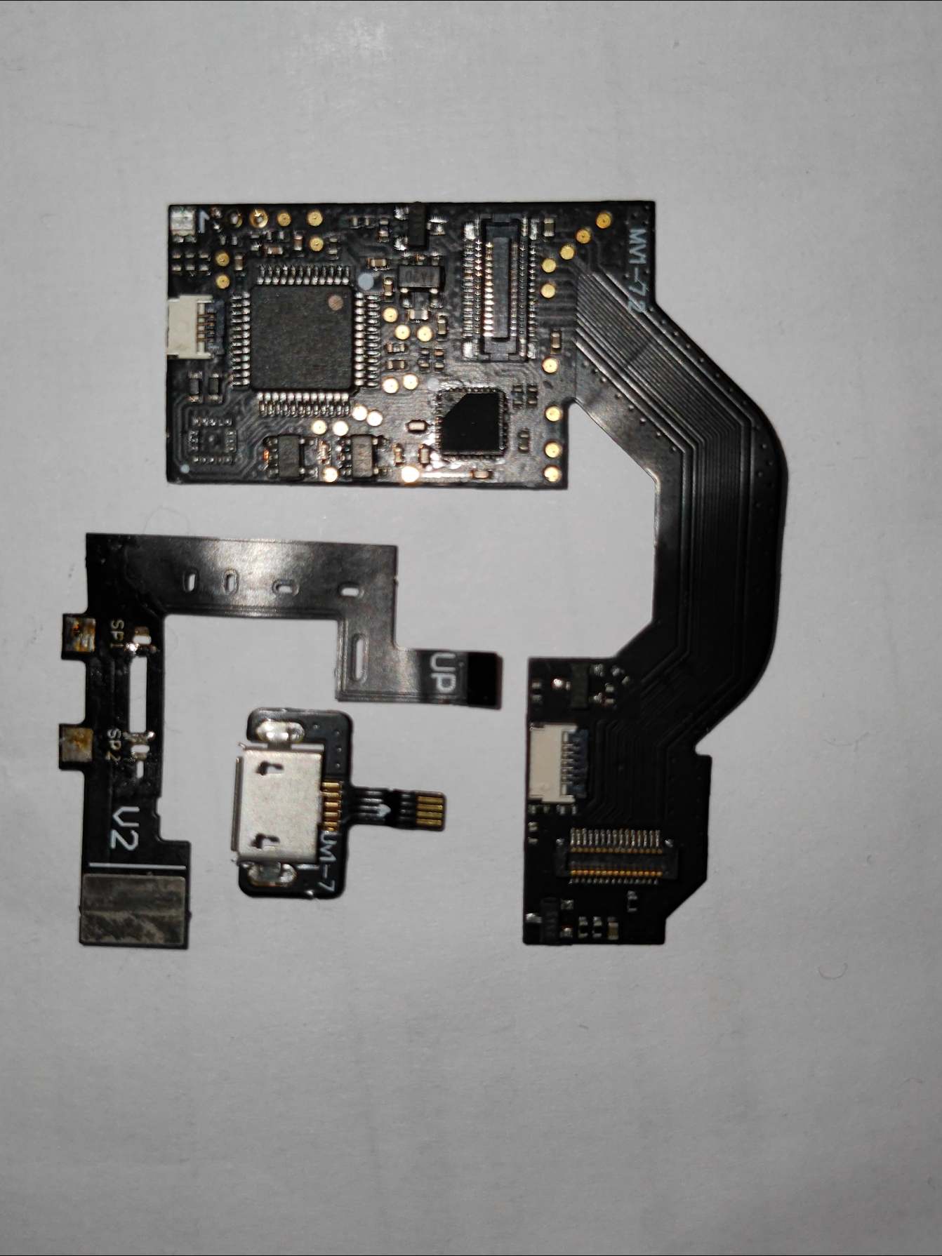
The battery was completely dead, so I picked up another (even the 9V battery trick that I’ve successfully used with overdischarged iPhone batteries didn’t work). IT SPRANG TO LIFE! It docked fine, charged fine with a genuine power adapter and I was so happy! Then I decided to do something stupid and install a HWFLY modchip. I was able to get it working on the first try (got that grey NO SD screen with the rocket that shoots with the power button)! Then things went downhill as I picked up a Nintendo licensed 128GB Micro SD card. The Switch have me a notice that it needed to update in order to up the card.

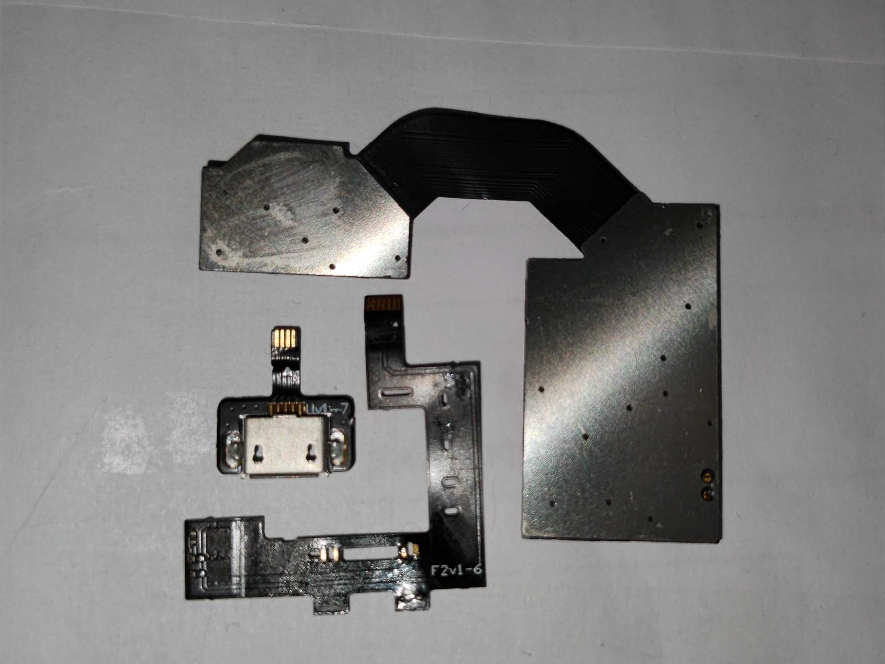
I thought “no problem” and let it do its thing. After a restart, I expected it to show the NO SD screen, but it booted straight into the original firmware? I kept trying to get the modchip to do its thing and no matter what buttons I held down, nothing worked. So I decided to try flashing the modchip. I learned that there was this one called “SPACESHIP NX” or something like that and used the one for my modchip. After finding a micro USB cable it liked I got it to be recognized by Windows and it flashed successfully. But the training lights kept going and going even after an hour and it was not as fast as it was when I first installed the modchip.

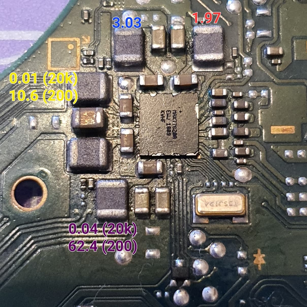
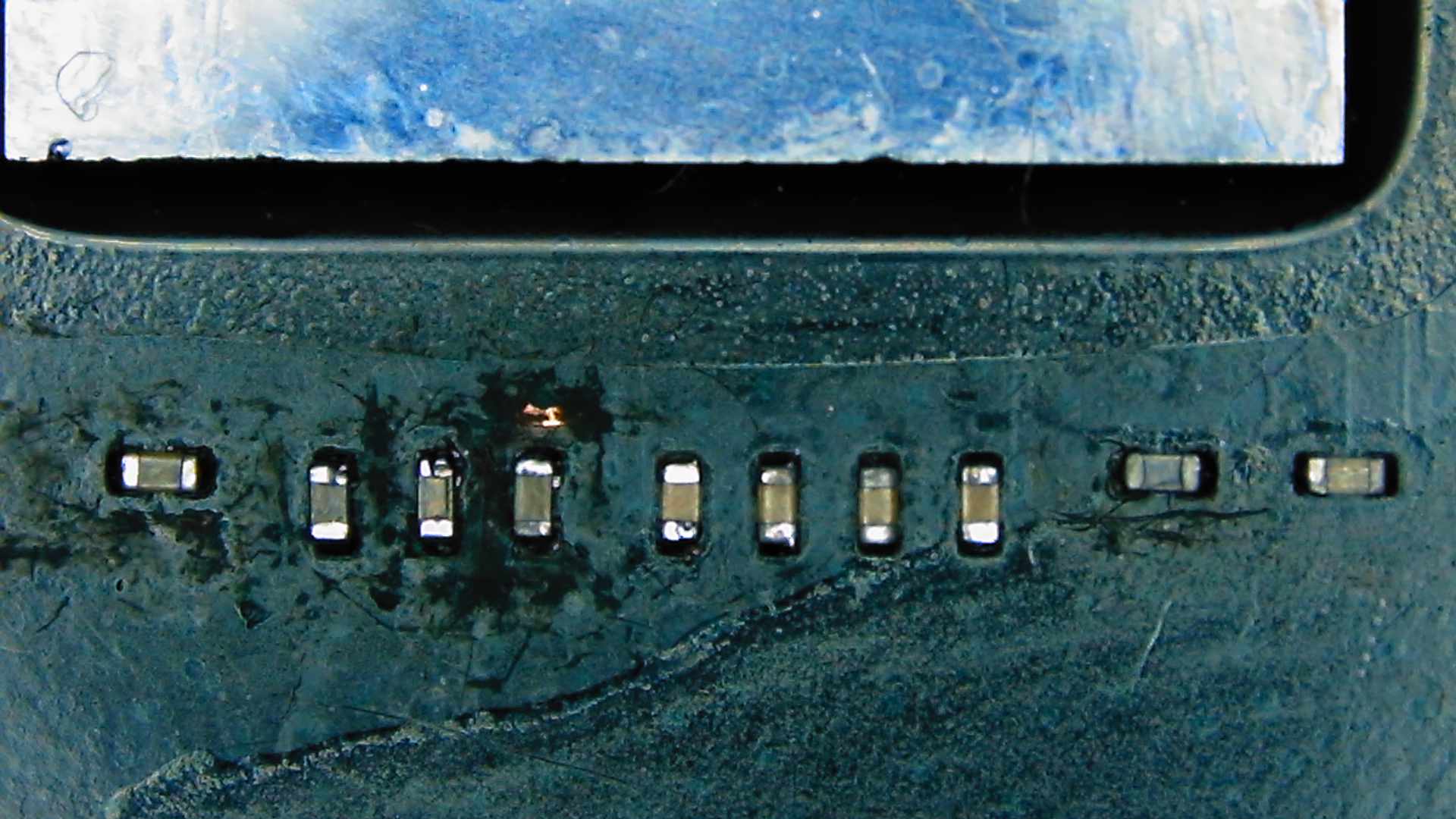
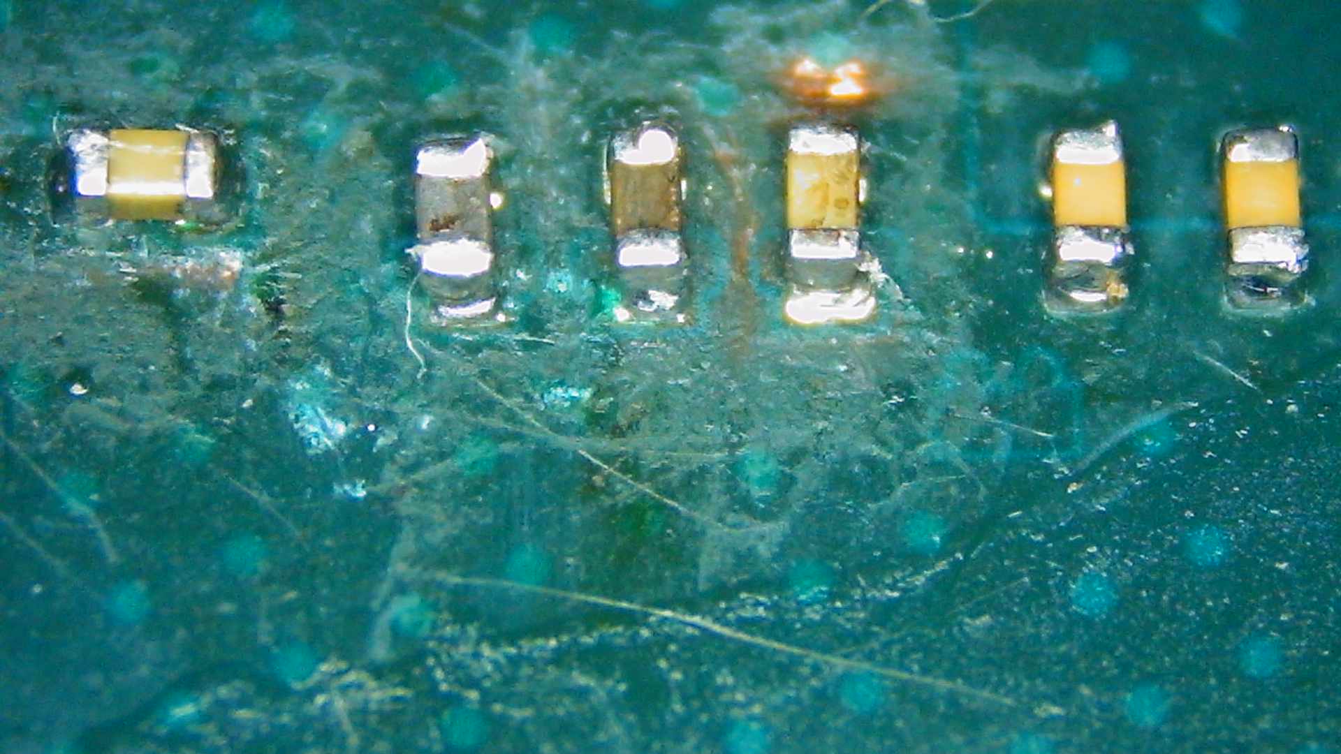
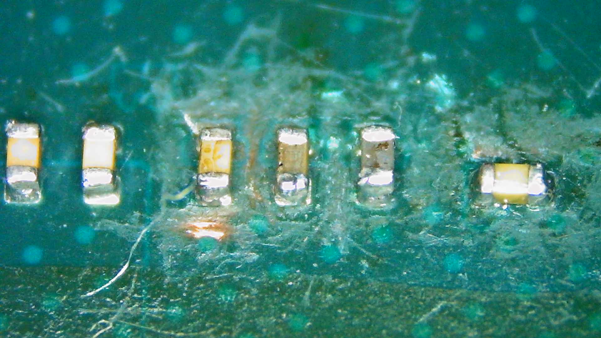
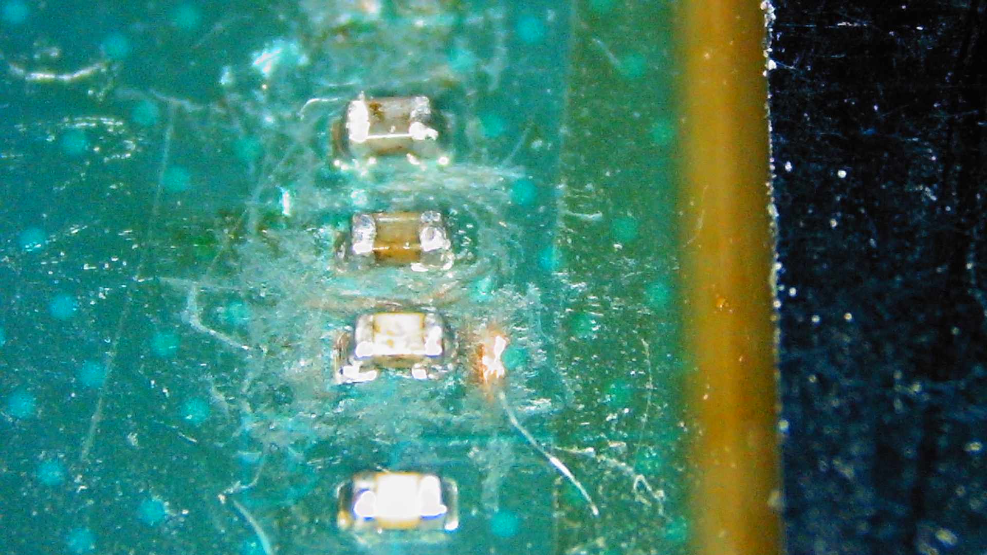
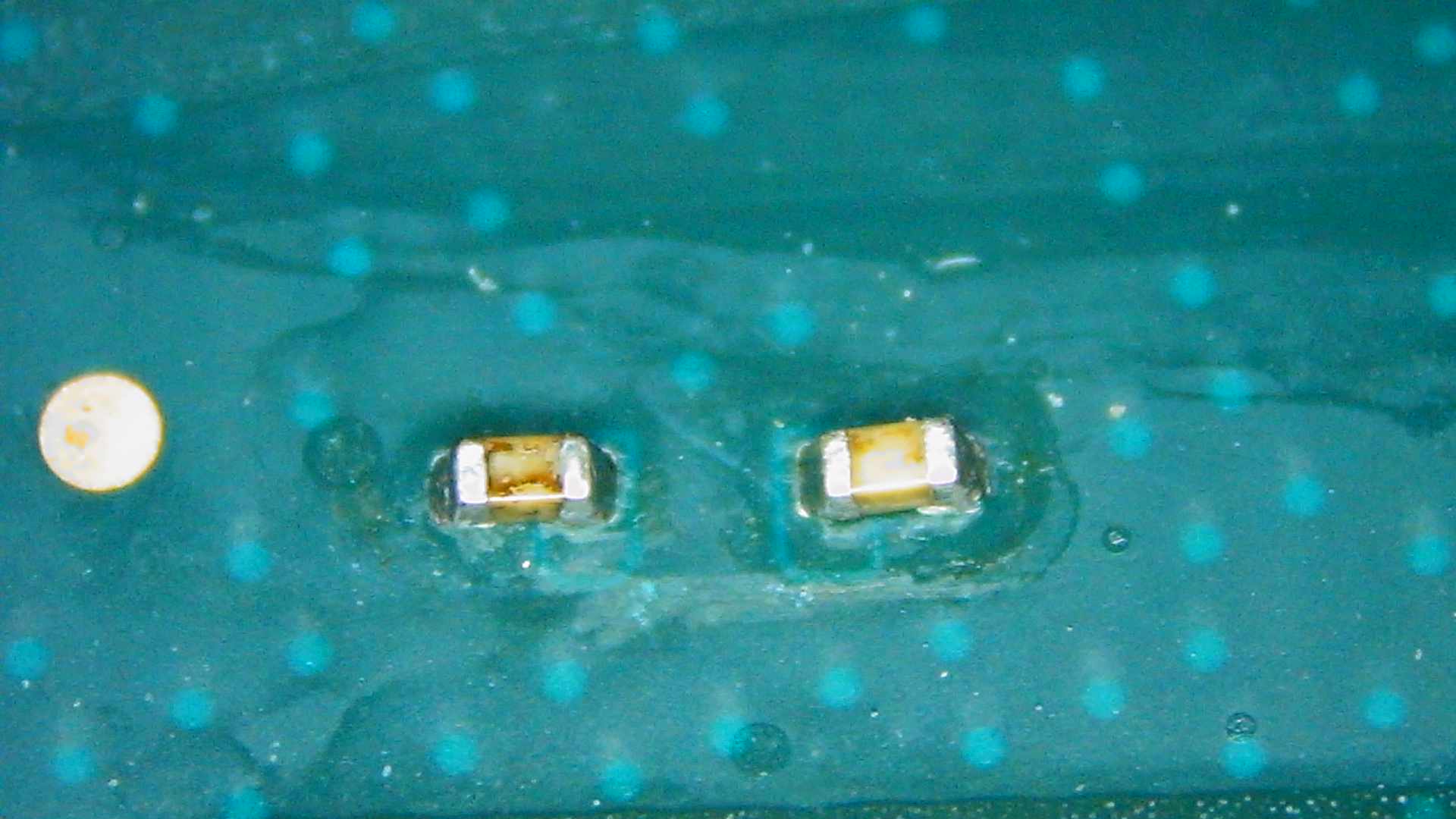
So I gave up and removed it thinking I could just sell the working Switch on for a good price. Now it won’t power up and I don’t know why! One of the capacitors looked a little iffy (SP1), so I replaced that with one from my donor board. Then I noticed that 4 of the capacitors on that row were shorted and I replaced them with donor and new 1uf capacitors. On Ohm mode (is that what it’s called? Anyway, I set it to 200k I think), with negative to the USB port as ground, all the ones I replaced now give a reading of 0.01. I have no idea what I did wrong and can’t see anything different, but I don’t have a clear picture of a working V2 board or even an idea what the correct readings should be.

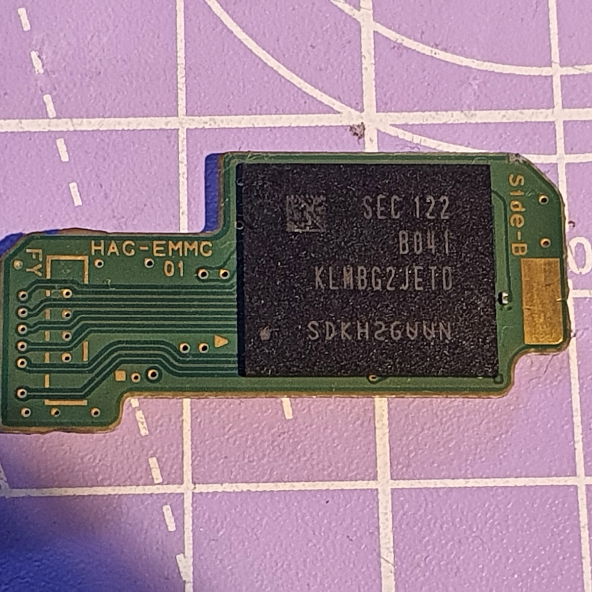
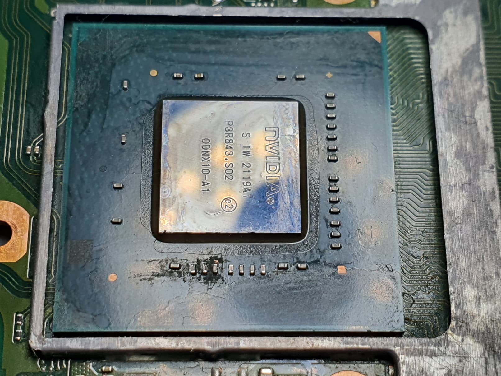
I’ve tried reflowing the APU and then replaced the MAX77812 as I’ve read that it could cause a no boot if faulty (M92T36 seems fine as I get 15v when plugged into the genuine charger). Still nothing except when the battery is connected to the board you can hear a faint “whine” like something charging up? I’m so desperate to restore this back to the way it was and just sell it, hopefully to someone not as stupid as I am to mess with modchips off AliExpress. Can anyone help at all? I have about 26 photos which I’ll figure out how to upload so I can make my issue as clear as possible.

Hope to hear from anyone soon! Thank you for reading ALL of this if you did!

I hope this is a joke… this isn’t a trick it’s just dangerous, once you’ve had a lithium battery explode in your face you won’t ever do this again… fun fact, water makes the acid react and burn hotter, so imagine how fun that’d be if it exploded in your eyes? - next time, just get a 5V USB to Li-ion/Li-po charger of ebay for like a quid and use that instead, and be patient. :slight_smile:

Can you provide a photo of your modchip for me (front and back) - the “hwfly” term gets thrown around interchangeably. I guess your talking about "Spacecraft-NX’ FW which afaik is meant specifically for the SX modchips (or the 1:1 clones, known originally as hwfly)

Also it’s worth noting that I’m pretty sure my 1:1 SX clone died straight after installing this Spacecraft-NX fw on my supposedly compatiable modchip… so there is that too :frowning:

Also when you say “V2” Switch, do you mean a Mariko rev?

Yeah, so you’d shift your meters range down so the the primary value is on the other side of the decimal place, “0.01” on the 200K range would be 10 ohms, so put your range down close to that.

Classic beginner mistake :frowning: :cry: …panic and make problems unintentionally worse. :crossed_fingers: SoC isn’t dead as a result.(that is if it wasn’t already)

So just for clarity bud, are we working on a Mariko board currently, the one that can’t boot after putting the modchip on it?

It’s all gonna be the same steps as the last few recent hwfly / picofly posts here I’d say, check them out and come back here with the measurments I asked for over there and we can atleast say if it’s worth continuing or just writing it off :frowning:

Hi there. Sorry about the late reply, I’m a carer so I’m always a little bit busy and do this “hobby” in my spare time. Lol, knew someone would harp one about the 9V battery trick! It’s something I learned online when dealing with mobile phone batteries. I’ve always been careful and it always worked for me as you need something just high enough to wake it up, so I speak. I’ve used the much higher current lithium RC battery packs in the past for other projects and haven’t blown up one yet (though I have a dedicated 12V Turnigy charger for those).

Anyway, I’ve been reading though a LOT of the posts you’ve commented in and I’m not quite sure what information you need. It seems that the photos I tried to upload didn’t work (even though I could see them, it kept giving me a weird error and wouldn’t let me save the post), so I’ll have to figure out another way to view them if they would be helpful. Is it just the readings of the capacitors on the APU or is there something else that you need?

It is indeed a Mariko Switch and it DID work after the modchip was installed, but then after the firmware update, the modchip just stopped working (would light up and all that but OFW would still boot up). When I removed the chip and replaced the SP1 capacitor as it looked a little damaged on one end was when everything went pear shaped. Could you just refer me to a specific topic that had everything you asked for and I can just go through that? I really do appreciate your time and I really wish I had just left it at repaired and sold it on instead of being greedy and wanting “fReE gAmEz!!!1!!!1”.

It’s nonsense… using a voltage over x2 the rated voltage of the cell does not magically “wake up” an over discharged cell. I’ll explain what’s actually happening, (on a well designed Li-ion battery) your 4.2V (max) cell is low (likely in UVP state), you connect you 9V battery to it, the voltage on your 9V is likely pulled low due the current draw of your patient battery, voltage on your patient climbs and gets ever closer to 4.2V, at which point OVP kicks on the small protection PCB and will effectively disconnects your 9V battery.

There is two main issues here with this method (again this assumes that the patient battery is actually decent quality and has the protection I talked about) 1: Protection circuitry speed in “disconnecting” your 9V source to the cell and 2: you are not regulating current to your patient battery.

Now Let’s looks at another scenario, the patient battery your charging does not have OVP, and yes, they exist and there are plenty of genuine iphone batteries and nintendo batteries on eBay like this (which look identical to the genuine) some might have simpler protection pre-cell, some might just have diode and a fuse. Anyway, in this scenatio, the voltage on your battery would climb to 4.2V and then… it will keep climbing, 5, 6, 7, BOOM!

In either cases, charging in an unregulated manner like this is dangerous, relying on the last line of defense (protection circuitry, if even present at all) is dangerous. If you want, try doing this with an electrorlytic capacitor, which while it doesn’t t use same chemistry, is very similar construction and the failure mode is incredibly similar, take a 5V rated cap and stick 10V on it, let it draw whatever current it wants (which is what your doing) and see how many seconds it takes before it blows up in your face.

Your conflating things here, which makes me think you truly don’t understand and I’d imagine is the reason your using the “trick” in the first place. Current is not really the primary issue here.

To safely charge an over discharged Li-ion/Li-po battery, all you have to do is limit voltage so it does not surpass the max voltage of the cell (4.2V in this case) and ideally initially limit current and trickle charge up to specified point… all of which a 1 quid 5V USB to Li-ion/Li-po battery charging PCB will do for you automatically (understand, your “trick” isn’t a trick, it’s dumb :slight_smile: it’s just doing what a dedicated charger is doing but in the most dangerous way possible essentially)

All the info you want is here in the below topic / thread :+1:

I really would just be going over the exact same stuff bud here, like a broken record :smiley:

Trouble is because you’ve replaced IC’s and reflown things (randomly) you’ve muddied the waters, you’ll have to tell me also how you conducted your replacements too (step by step) just so I can be sure they aren’t going to cause issues (assuming the measurments your going to take from thaty topic as reference, are in the realms of ok)

OK, OK, so it’s dumb. I get your point already! I’ve only done it a few times and it’s always been with genuine batteries anyway (since I’m apparently still here and haven’t blown myself up yet. Just temporarily working with what I had at the time). This Switch if I can revive it will be the last of these devices I want to work on. I’ve repaired many handhelds, phones and tablets, but there was much better documentation on those compared to this one. Seriously, finding information on Erista models was way easier that Mariko (I only call them V1 and V2 in case others who don’t know the codenames and might’ve experienced my issues could find a solution (if it’s salvageable) or possibly be kind to chime in with what works for them. V1 and V2 are more common on a Google search, trust me on that.

I didn’t do it randomly (well, not intentionally). I checked here and sites like Retrosix for any ideas on what could’ve died because of the modchip or the update, or whatever. I still can’t understand why the firmware update (16.0.3 I think) killed everything as when I looked as the solder points everything was still attached perfectly. The modchip just refused to do anything and when removed just killed everything, no matter how careful I was. Ill follow what you suggested in that post and report back. Thanks for that. I’m gonna try to upload a couple of pics of the “core” modchip I used:


Understand, me telling you all this isn’t to be mean or to “harp” on, it’s just to let you know and perhaps let anyone else know who reads this topic. If I don’t say anything, then that’s one more person potentially using the “trick” :slight_smile:

Some people relate that to the board names (which doesn’t work), some people relate V1 to unpatched Erista, and V2 to patched Erista. The only reason why I was asking for clarification :+1:

Yeah not your fault :frowning: check my thoughts here on this

Does the big chip in the middle say “GD32XYZ” or something along them lines? (or if you can capture the part number in the photo?) Just curious as to what version this is, I think it looks the same or very similar to the one I had (years ago in my case)

I know you’re only telling me for my own good and I’ll be sure not to do that again and cough up for the proper equipment. Thanks for watching over me and others that may make the same mistake! Thank you for the explanations as well. It seems very simplified online where decent lithium batteries just go in a sort of zombie state where the voltage is too low to accept anything. And by using a higher voltage input (briefly!) can get it out of that state.

I will admit that I have been either very lucky or good with my hands (and sometimes common sense) in that I saved a fair amount of electrical items. This is my first Switch however. I’ve attached a pic of the component on the modchip as you requested:

I am a bit thick when it comes to the primary rails and even after searching the forums I can’t find where you explain how to test them (was ready to go to Retrosix Wiki for that!). I know there are test points on the board, but I don’t really know what goes where. I remember there was a guide for the USB C port pinout and where the corresponding points are on the board. Is this what you are talking about, or am I completely off? If I’m on the right track, I do have a double sided male/female breakout board that can make testing easier…

Yeah the internet is the land of Chinese whispers and conflation and confusion :wink: assuming the battery has decent OVP, then, the cell would/should never see the “higher voltage” so thats that theory out the window :smiley: . What I think this has been confused with, is, cells which don’t have protection or have minimal protection (which I touched on) such as a good majority of 18650’s - the cases which I think you’ve seen confused with, are not simply over dishcharge but further along than this… I’m no chemist, but I think it was something to do with the crystal structure of the electrolyte failing :man_shrugging: which could potentially be resolved by pulsing at a very high frequency (we’re probably talking microseconds here) a very, very high voltage to break it down… but even this has been largely proven to not work or be temporary or cause damage / dangerous scenarios, so yeah, reckon probably a bit of Chinese whispers going on in internet land :smiley:

So this does indeed seem to be a clone of the SX modchip, so the Spacecraft-NX FW should have in theory worked on this. I don’t recall if Nintendo actually ever went out their way to detect these modchips (or any modchip variant for that matter) and/or brick them or the console… It would be fairly easy for them to do this given the way these modchips modfiy the EMMC data.

No worries, I am too in most other areas :wink: all the info you need is in the picofly topic I linked you to, including all the locations (which the OP is finding and posting) and how to measure them :+1:

OK! I think I figured it out now! I had to look really hard on the forums, but I found where you mentioned primary rails and even took a picture (wasn’t the same topic you mentioned though). I copied it and did my best to get the readings (done on 20k setting unless stated otherwise). The multimeter I have is a UNI-T UT33D (not all of us can afford Fluke!). I’ve also taken a couple of pics of the EMMC as well.

The difference between my issue and the OP in the picofly topic was that mine WAS working fine completely assembled and I put kapton tape over the EMMC and also on the area on the metal plate (is that a type of EMI shield?) where it would contact the modchip. I’ve read that some people got away with firmware 16.0.3, so maybe I was just one of the unlucky ones?

Also please forgive how the MAX chip looks, it was me trying to grip it while using hot air. I DO have a tool for lifting ICs, but I was trying so hard not to touch all those teeny capacitors and stuff around it lest they disappear into the great unknown! I have a bad feeling the SoC is well and truly dead though. Also I have another problem even if it isn’t…


Good stuff, this is a few of them :+1: (I’ll come back to your readings at the main PMIC in a mo)

The locations are indeed in that topic (as well as some aditional areas to measure also) - I described the locations, and the OP eventually found them and took the readings

Don’t worry about it, fun fact, pretty much all Fluke meters within the 200 quid range are actually terrible meters anyway, based on 20+ year old designs, maybe half decent for an electrician, terrible for us.

K, in regard to your readings at the main PMIC inductors, if I’m understanding your meters readout is showing

blue 3.03K,
red 1.97K
purple 62.4ohm

Red is in the realms of alright (on some meters)
Blue seems on the low end
purple is on the low end (somewhere between 40ohm and 62.4ohm)
Yellow is just about fine (for Mariko)

Don’t worry, I’m not really concerned to much with the slight differences in cause, I was more pointing towards the requirement of getting the rail measurments more than anything (I think you also might be confusing two very similar topics which is linked in the one I linked you too, as the modchip was working in the case of the OP initially : confusing stuff)

In regards to your main PMIC, did you replace this, or? can you tell me step by step what you did with the PMIC here just so I can understand and better help you for next time. The PMIC in it’s current form is likely dead I’m afraid and will need to be replaced. Not too worried about the damage to the polymer (black) top, but I am about the chips/cracks in the die / body of the IC.

Also, if you can, can you take a picture of the SoC for me too

You know, being a noob and all, when the Switch still refused to power on, I read that the MAX chip there could be the/part of the issue. I swapped it from the donor board. I don’t see the crack in it, but when I used 99.9% isopropyl alcohol to clean the flux residue, that weird curved line comes up. I had gotten rid of it, but then it came back when I saw more flux to clean off.

I’m happy to replace it as I don’t fear BGA soldering that much (all depends on the size). I use a 183C leaded solder paste (I don’t do any lead-free crap). Fun fact: I was so glad that the iPhone 8 Plus BGA stencil I have works with all the BGA components I’ve replaced so far. As for the SoC pics… you’re not gonna like them. They were what I tried to upload on the first post. I found a few of the SoC capacitors shorted in continuity mode and hoped that replacing them would solve the no boot issue.

I got them on great the second time round (where they didn’t look bridged under the microscope). Still wouldn’t turn on, so I stupidly removed them and put new ones on and they just started looking worse and worse. The scratched up surface was just me fighting with moving these super tiny things around with a fine tipped soldering iron (can’t remember the name but it has a curved tip):


Right, this is the problem with those silly guides we talked about, they present very little info, say things in the definitive (as though it’s fact even if the info is wrong) and send beginners down rabbit holes :frowning: For next time, so you know, there has to be a reason behind doing something (in this case changing the main PMIC) - So, measuring the rails (voltage) it generates might be a good first step (at it’s output inductors) and while that’s handy info to have, the info gained from this is limited (it’s not really telling you much outside of, the voltage is present and the PMIC is able to maintain it at a given current), so next we’d check the PMIC rails resistance to ground to see if there is anything dragging any of them down, which may point to other things on the board which rely on said rail/s, or, if multiple rails generated by the PMIC are dragged down, then we can narrow things down and say it’s more likely to be the PMIC as a result of the commonality (or the SoC in that instance too) - only then would you consider pulling the main PMIC but much like a detective, one piece of evidence is never enough, it’s better to get multiple so the case is a slam dunk :wink:

Also, reflowing is never going to be a solution, ever, in these sorts of cases. The only time reflowing something is ever going to help, is if your in a liquid scenario and there is crap under a chip and your trying to flush out (which is honestly not great practice) or if an IC in question has bad solder joints, none of these would be the case in your instance, and reflowing puts things in danger (particularly the SoC which is heat intolerant at the die) - Just telling you this so you know for next time :slight_smile:

If you look bottom right, there is a chunk out the corner, middle right at the bottom looks to have a gouge, top right looks to have an indent or hairline fracture. Tweezers are half the issue on chips like this, decent pair will work fine :slight_smile:

Good stuff :+1: after you’ve taken the IC off, and wicked the pads, can you take those same measurments again on the surrounding inductors so I can confirm.

:+1:

J type of some description I’d imagine, yeah you’ll struggle with a tip like this given the thermal mass on the wafer, tip: you can have your hot air help out in situations like this while your soldering, wave your hot air in the vicinity at approx 150C low ish air. Sometimes also, it’s easier just to wipe the caps off completely to take them out the equation during troubleshooting (the are just bypass caps after all and won’t ordinarily prevent boot)

Have another skim over that other topic I linked you to earlier and find reference to 3V3PDR and the other Max IC below the SoC where he took measurments (and photos) and if you can do the same too, for further clarification

Also, if you can, can you confirm the colour of the resin round the SoC die, is it a blueish greyish colour or is it a brownish colour? bit hard to tell as I think shadows are being cast in the photo

Actually, I missed this one :frowning: this is kind of what I was afraid of, resin round the die becoming discoloured / brown :cry: this is typically a good indicator that the SoC is now dead as a result of the heat… though we did have one guy recently on the forum where we persevered and the console worked in the end (albeit with some caveats and signs of dread in the future) so I’m happy to help you continue on if you want as a learning exercise but I’d just say, don’t get your hopes up, and if we can get it working, don’t expect it to last long :slight_smile:

I had a feeling I’d kill it… I’m willing to mess with it for fun, but I still want to know why it died in the first place even before I killed it further. Did Nintendo’s update really kill it? Maybe if I didn’t try to reflow the SoC, it would’ve been worth it.

I’ll probably won’t mess with a Switch again (in fact I managed to acquire a Microsoft Surface Duo 2 phablet that I would like to try emulation on (Snapdragon 888), but I would love to do a couple of mods on it first (upgrade the RAM and work on a new housing as the glass is killing me and doesn’t help with thermal throttling).

I’ll continue working on it tomorrow and send you the information you need if you’re still happy to help. If it isn’t salvageable, I might just see if another faulty one shows up again on eBay with a broken screen or something and just swap the good parts over?

Yeah we can try and get to the bottom of this, though it’ll be a bit harder to tell if the SoC is fully toast.

Current theory atm is, based on the problem occuring following HOS update - The modchip presumably only modifies the EMMC data (boot0 partition) if it is changed, which we can assume did during the HOS update which is expected ordinarily (unless the modchip somehow prevents this) , then the modchip would afaik then attempt to modify the boot0 partition once again. and something has happened here tbd

Excluding potential EMMC partition issues (boot0 problems preventing boot or data corruption potentially caused by updating HOS)

This is a bit of a question mark for me, I have some very very vague memory back in the SX days (before they got locked up) we did have to wait and update the modchip FW before updating to the latest HOS version (though I could be remembering wrong and I don’t recall the outcome if you did actually update HOS) - given that SX is pretty old at this point, and given that the clone your using is using FW which I think is over a year old, I suppose it’s possible, maybe, though, I don’t think it messed up the modchip back then. but I do recall, after I installed spacecraft-nx FW on my modchip that was the final nail in the coffin for my modchip (I even replaced the GD32 MCU on it and nothing, think it killed the fpga/cpld on the PCB) maybe because it was a clone :thinking:

I’ve not worked on these, weren’t these the nightmare ones to get into? or was that a different model?

Sure :+1:

Sure, don’t see why your patients Switch screen assembly and other misc parts would be bad.