I’ve just installed a modchip into my Mariko (v2) Switch. Now it boots into hekate but everytime I try to boot into OFW or Atmosphere, the system would freeze after the first logo.
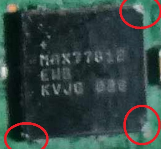
I’ve opened up the console and found out the MAX77812 ic got very very hot after the first logo boots. Also the 2 circled caps are shorted. Any ideas what’s wrong? I can do everything inside hekate except boot past the first logo.
Here is the image: imgur com/a/evqOs0s
Maybe a trick of the light, but based on the image you provided, looks like you’ve damaged the IC and chipped 3 of it’s corners. Me personally, I’d swap this IC prior to anything else (but this is up to you… I just wouldn’t be happy leaving it like this even if it does end up infact working with this IC due to unrelated issues elsewhere.) I’d also provide photos of your install so we can look for issues elsewhere, as well as components surrounding the SoC shield frame
I got a photo of the board before I went to my relatives house (currently not at home atm, I’ll be back a few hours later) and there were no shorts elsewhere. The only symptoms is the max chip burning up (it actually burned my finger lol)
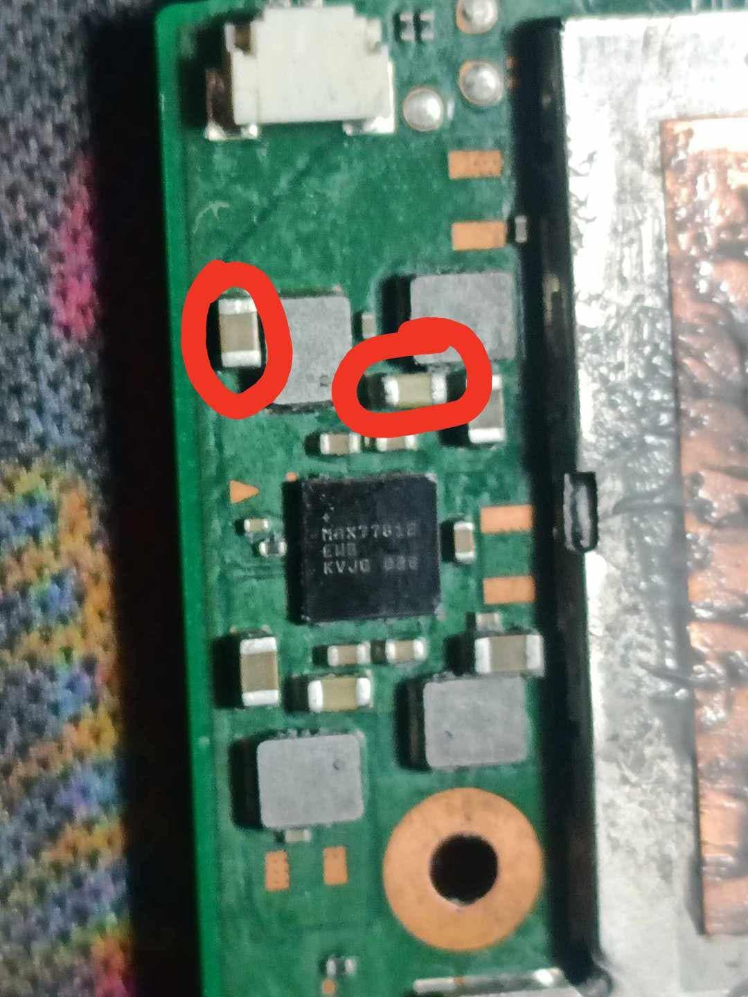
Here is the image of the full board: imgur com/y7WTQgr
The cap closed to the edge I have 30-ish ohm to ground where the middle cap I remember it connects to Vsys which means should be more than 100 ohm to ground.
If you have the max77812 stencil, you can remove the chip and check the resistance again.
You sure about this? pretty sure this cap is on the same rail (Secondary CPU rail) as the inductor next to it, so would expect somewhere around 11 to 17 ohms relative to ground. Or are you measuring reverse polarity maybe?
I personally would as it’s physically damaged by the look of it, it’s getting hot, usually go hand in hand (but depends on your your level / confidence reballing etc, so you might wanna narrow it down further first) You could check the resistance to ground on your SYS rail as Jkyoho mentioned.
I’d be careful using this terminology (becoming a bit of a bad habit / trend ) there is at least another 20 other IC’s on Switch which use this terminology for completely unrelated I/O / rails. Be a bit like me saying, check your 1V8(PDR) by referring to it as VDDIO, which again, another 20+ IC use this terminology, and much like “VSYS” are completely unrelated and can have vastly different voltages. And to add further confusion, there is another 5 at least, completely independent 1.8V rails completely unrelated to one another . This is one of the reasons schematics and boardviews use a completely different naming convention as compared to the naming used by a particular IC(from datasheet)… Hence, why you see me calling rails things like, SYS, 1V8PDR, 3V3PDR, etc , this way, they cannot be confused with anything else, or other rails at the same voltage level (of which I’d assign a different name) This just so happens to have the positive side effect they are more easily searchable too - I only mention this bud, as I’ve had a spat of boards in the past year where I can see beginners having a “AHA!!” moment, after reading some IC’s datasheet and thinking they haven’t got continuity from some Rail/IO to another and then they jump it (as evident by solder work at these I/O etc in question) and kill the SoC or other (which I think the retrosix guide isn’t helping with)
I should have said Voltage from battery on mainboard instead of refereeing the same ID(Vsys) from MAX77812 datasheet.
FYI, you might be refereeing 14ohm to ground on 0.85V line from MAX77620H v2 boards,where this MAX88712 LX3 LX4 is GPU core voltage only
I just measured the 23 ohm on the 0.8 line from MAX77620H(14 ohm normally). So I guess it just the variation between boards. At least it wasn’t 40+ ohm like v1 board.
Nope, I wouldn’t get it mixed up with a rail produced by MAX77620H (as the CPU rail generated here is for the boot CPU, has nothing to do with the secondary CPU rail) But…I may have muddled the [secondary] CPU and GPU rail generated by MAX88712 though
Guess White or black from the image in that post would be the other (can’t remember) . Have you verified which is which yourself by tracing back to SoC pads yourself? as seems more locgical to me that 57 ohm reading (white) would be the GPU rail
I didn’t trace the rail to SOC, but from the boot sequence/voltage present sequence, LX3(black) 1st(when power on triggers), LX4(white) next(1st logo shows), then LX1&LX2 come up last(when 2nd logo shows)
Yeah, not sure you can rely on that, as the second logo will corelate with the approx time of both the secondary CPU rail aswell as the GPU rail too.
Sidenote: internal graphics seems completely independent (hence why we still see the first boot logo, Hekate grahical UI etc etc) even when the GPU hasn’t come up
just by correlating it with a regular rev Switch - Makes the assumption the capacitor order is the same (left to right) on the SoC itself
(and of course, if anyones curious, modchip flex is connecting to the boot CPU (or CPU(1) rail if you prefer) rail.
No Idea what purpose the unmarked rail is serving (the inductor top right :thinking) … maybe standby voltage when other rails go to sleep (?) - I should have cross correlated it too with the original rev… oh well
Sidenote: I’ll refer to SYS (VSYS) from now on as PSYS to avoid any potential confusion elsewhere (even though “SYS” is rarely used on pin markings for a given IC, there is a chance I suppose… much like VSYS, so best to be safe than sorry I guess)
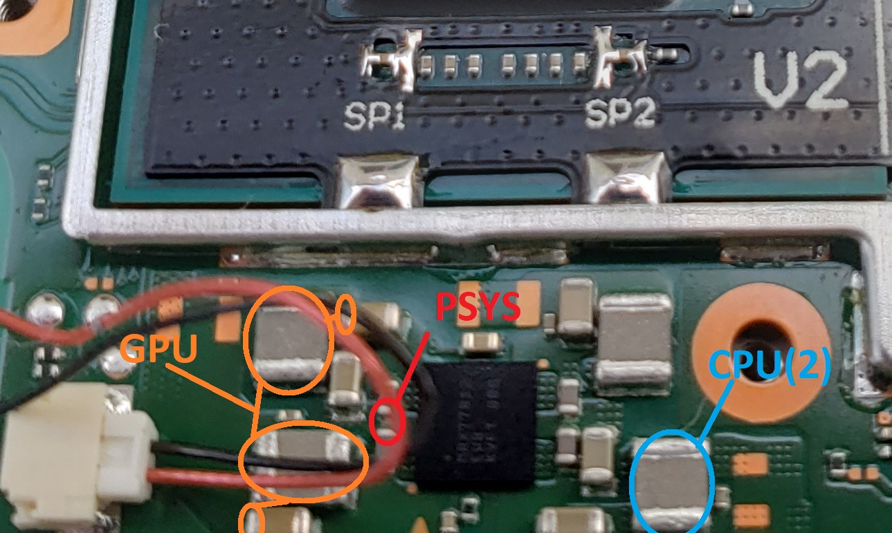
So I found something on the APU that made my heart sank. A solder blob shorting 2 caps next to the SP1. I’m going to try my best to remove it, hopefully the APU isn’t fried at this point.
I’ve cleared the solder blob, which changed nothing and the 2 caps next to SP1 are shorted. Are these shorts caused by the max chip since I haven’t pulled it out yet? Or is it the opposite (APU causing max chip to get hot)?
The 2 shorted caps on the APU looks kinda iffy so that could be the problem.
Update: I’ve found 2 more caps shorted on the other side of the APU marked red.
Sorry for the late reply as I needed to wait for the next reply.
Image: Imgur com/a/IEFQTZl
Measure resistance to ground at PSYS and CPU(2) and let me know the actual resistance (telling me “short” doesn’t really help anything) also photos of your install